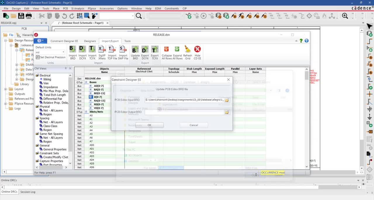
Constraint Designer EE allows you to easily define design constraints. Constraint Sets can be created and assigned for physical routing, vias, target impedance and tolerance, min/max propagation delay, differential pairs, and more.

Eliminate errors due to miscommunicated design requirements by assigning constraints at the schematic level and embedding them directly into your design database.

Automatically bring design constraints into OrCAD PCB Designer for easy design and analysis. Sync with PCB or schematic at the touch of button for seamless bi-directional communication.
Communicating design intent is an important aspect of any project. With designs increasing in complexity, ensuring information is accurately relayed can be a challenge. One missed piece of information can lead to a cascade of incorrect design decisions, often not found until later stages of the design cycle. With Constraint Designer EE, easily define, communicate, and manage design intent by making design rules an inherent part of your process. Now you can be confident knowing design intent and information is relayed accurately, allowing you to make intelligent design decisions and avoid costly headaches.
With time to market a crucial aspect of any design, reducing time spent on monotonous tasks is vital to the success of a project. With Constraint Designer EE, you can save time by creating and reusing rule sets throughout your entire design.
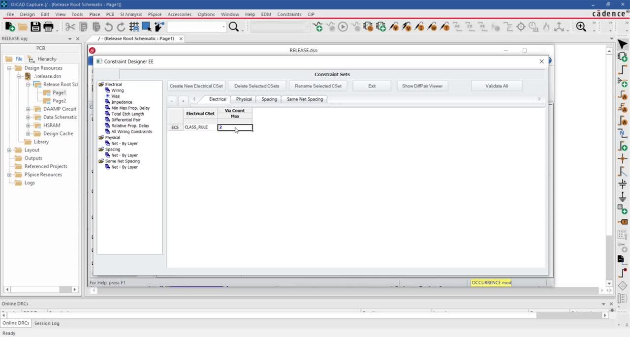
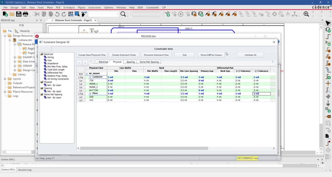
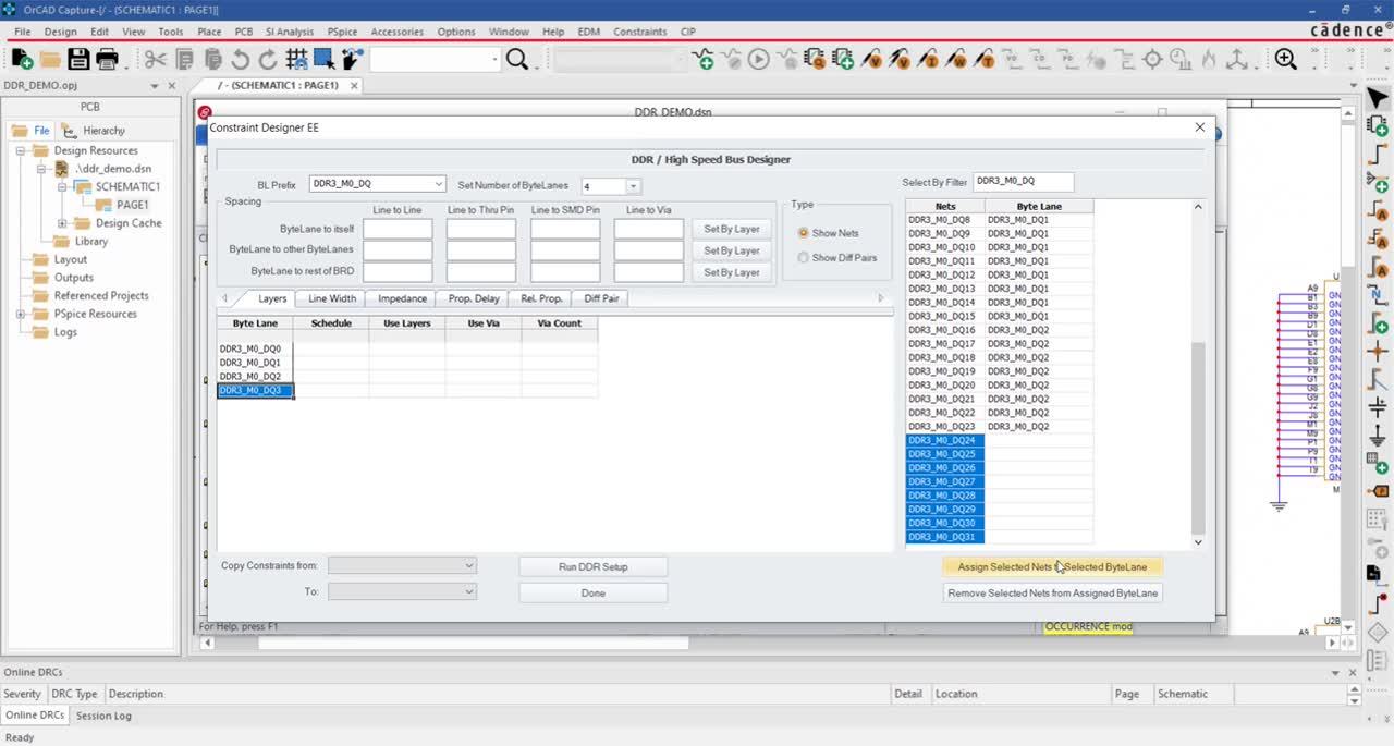
Routing DDR and high-speed bus interfaces can be one of the most daunting tasks in your design. Just getting all the various signal relationships and requirements defined and understood can feel like a PhD thesis on its own. With the new bus designer, all you need to do is simply describe the bus you are trying route and Constraint Designer EE will handle generating the appropriate constraints automatically.
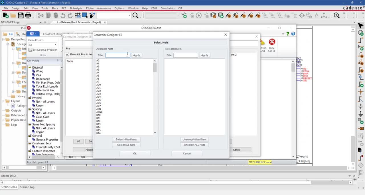
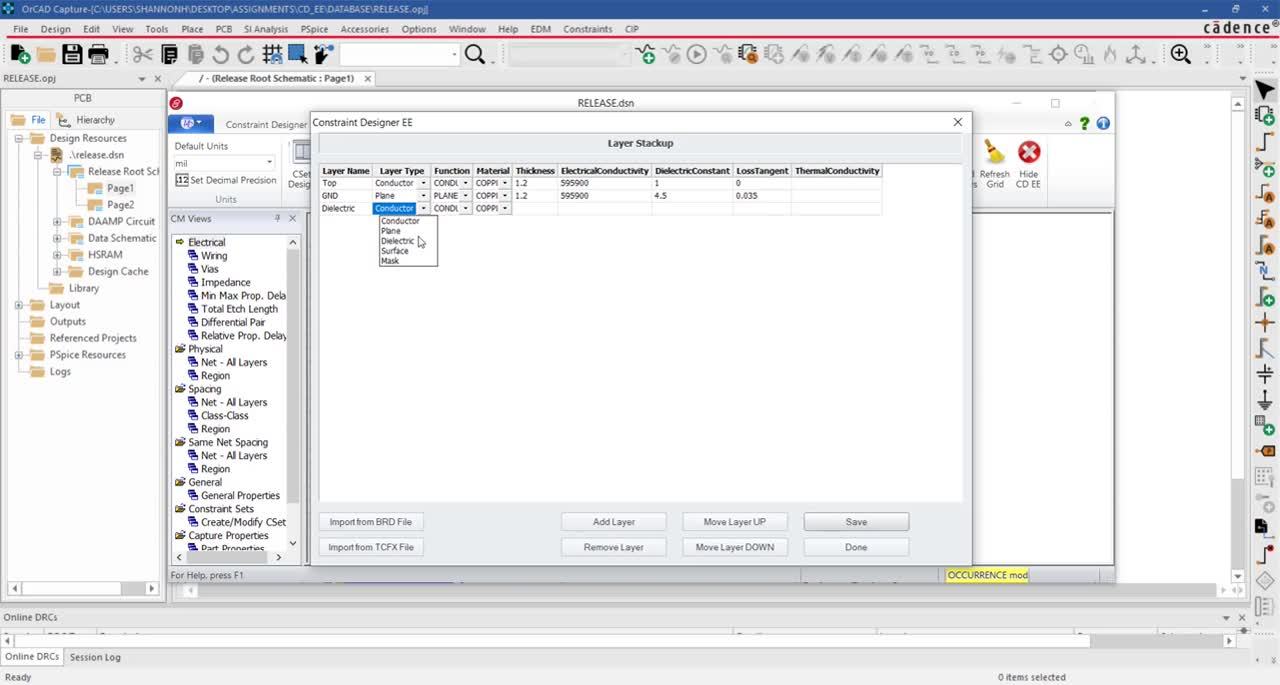
Defining the design specifications at the schematic level, will result in less room for interpretation in the PCB layout. With multi-layer boards, rules become difficult with spacing, line-width, and rules for diff pairs or DDRs defined on a layer-by-layer basis. With Constraint Designer EE, you can create detailed, layer-based rules and accurately communicate your design intent from schematic to PCB.
