Rules or constraints are critical to define how aspects of the design should be completed. If rules are not applied accurately and reviewed during the design process it can lead to incorrect operation, an unmanufacturable board, or a complete redesign; especially as designs increase in complexity. With OrCAD X, you can use constraints and design rule checks to:
- Adhere to device design requirements
- Guarantee proper functionality
- Ensure safety
- Improve signal integrity
- Adhere to manufacturer’s capabilities and requirements
- Verify the PCB assembly
This how to will provide step-by-step instructions on how to use constraints and design rule checks in OrCAD X Presto.
To follow along, download the provided materials above the table of contents.
How-To Video
 Open in New Window
Creating Electrical Constraints in OrCAD
Step 1: Select Tools > Constraint Manager from the menu.
Step 2: Select the Electrical domain from the Worksheet Selector.
Step 3: Select the Electrical Constraint Set > Routing > Differential Pair worksheet.
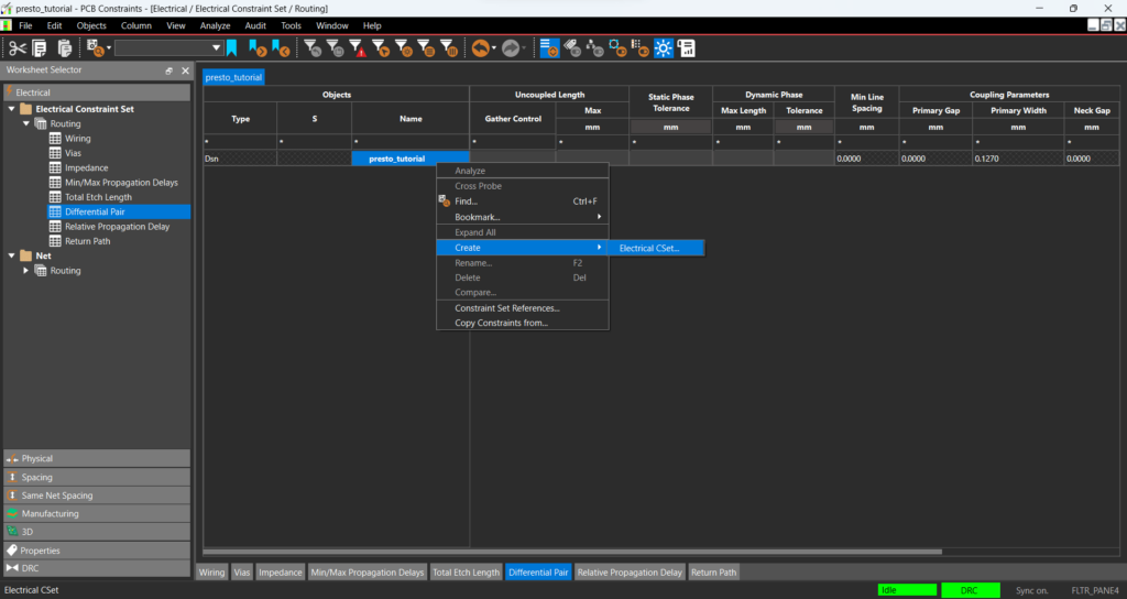
Step 4: Right-click in the table and select Create > Electrical CSet.
Step 5: Name the CSet DP and click OK.
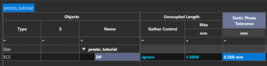
Step 6: Enter the following values for the new constraint set under their respective columns.
- Gather Control: Ignore
- Max Uncoupled Length: 5.08
- Static Phase Tolerance: 0.508
Step 7: Expand the Net > Routing > Differential Pair worksheet.
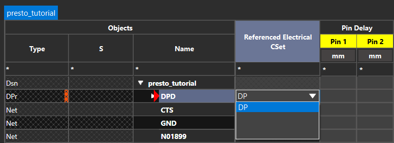
Step 8: Select the DP CSet from the dropdown in the Referenced Electrical CSet column for DPD.
Note: Assigning the constraint set at the top level of the differential pair will assign the associated rules to each net in the differential pair. Need help configuring differential pairs? View our how-to here.
Creating Physical Constraints in OrCAD
Step 9: Step 10: Select the Physical domain from the Worksheet Selector.
Step 10: Expand the Physical Constraint Set folder and select the All Layers worksheet.
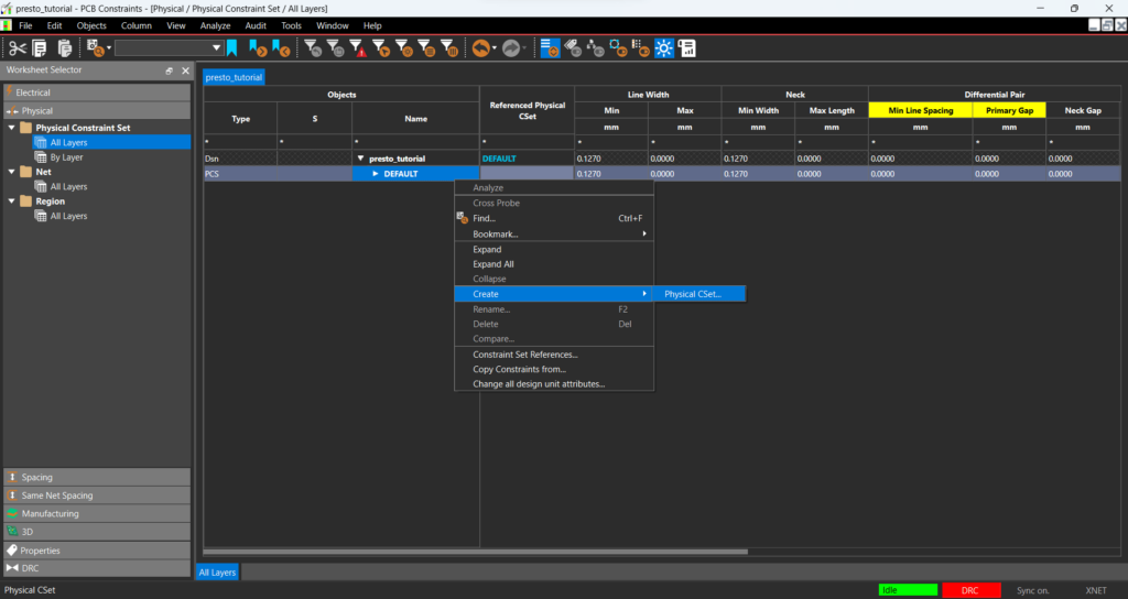
Step 11: Right-click the DEFAULT constraint set and select Create > Physical CSet.
Step 12: Name the constraint set DP and click OK.
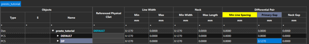
Step 13: Enter the following constraint values for the new CSet under their respective columns.
- Minimum Line Width: 0.127
- Primary Gap: 0.127
Step 14: Select the Net > All Layers worksheet in the Physical domain.
Step 15: Select the DP CSet from the dropdown in the Referenced Physical CSet column for DPD.
Activating Constraints and Design Rule Checks in OrCAD
Step 16: Select Analyze > Analysis Modes from the Constraint Manager menu.
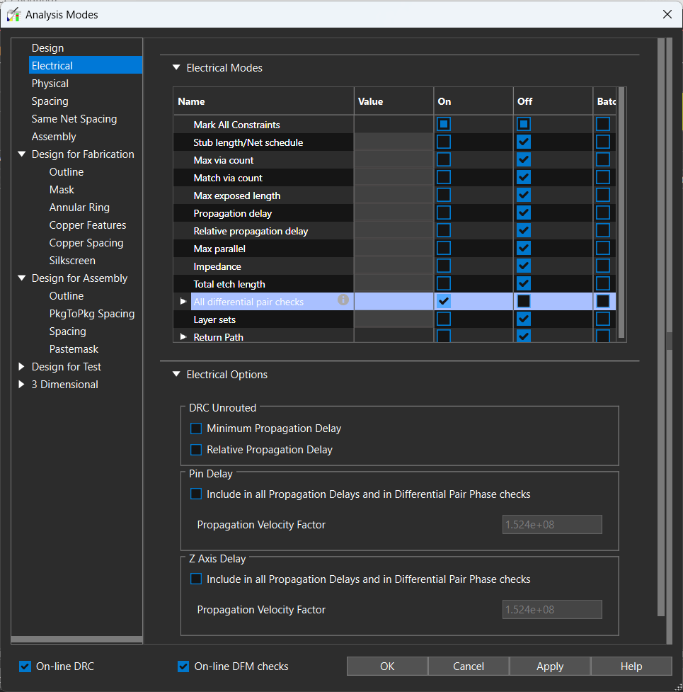
Step 17: Select Electrical from the Analysis modes list and check the box for all differential pair checks to turn on constraints for differential pairs.
Step 18: Select Apply and OK.
Step 19: Close the Constraint Manager window.
Confirming the Constraints
Step 20: Back in the Presto canvas, in the Properties panel, select All Objects to turn off all objects then select Nets to filter only net objects.
Step 21: Select net D- from X1 or IC1.

Step 22: Select the Constraints mode in the Properties panel. The physical and electrical constraints for the differential pair are shown.
Step 23: In the Properties Panel, select All Objects under Selection Filter to turn all objects on.
Routing with Constraints in OrCAD
Step 24: Select the Add Connect button on the toolbar.
Note: If the add connect button is not visible, right-click on the fourth button down to view the other available commands and select it.
Step 25: Select one of the pins of the differential pair. Both nets are activated and routed together.
Step 26: Click to place the trace on the PCB canvas as needed.
Note: Zoom in and out of the board as needed with the + and – keys on the keyboard, respectively.
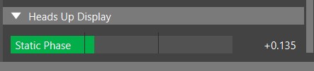
Step 27: Scroll down in the properties panel. Here you will see a heads-up display that provides real-time feedback on adherence to constraints during routing.
Note: Any traces that will violate constraints are highlighted in white while routing.
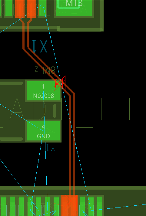
Step 28: Click to complete the routing. Any design rule violations are flagged with a DRC marker.
Step 29: Select the Arrow icon from the toolbar then select a blank space in the PCB canvas.
Analyzing Constraints and Design Rule Checks in OrCAD
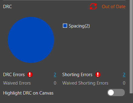
Step 30: View the Status section in the Properties Panel. Any DRC violations are reported in a pie chart.
Note: If the DRC is Out of Date select the refresh symbol to update the design rule check.
Step 31: Select a section of the pie chart or the hyperlinked DRC errors reported to open the search panel. This will display all the DRC errors for easy location and review.
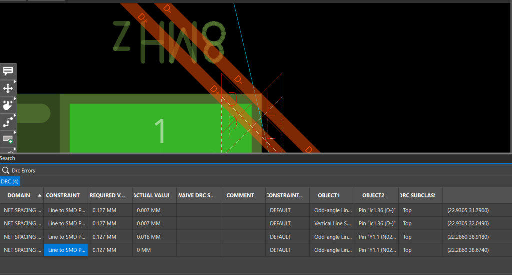
Step 32: Double-click a line item in the search panel to be brought to the location on the PCB.
Correcting DRC Errors
Step 33: Select the Slide icon on the toolbar.
Note: If the slide icon is not visible, right-click on the third icon from the top and select the slide icon.
Step 34: Click to select a trace of the differential pair. Move the mouse to the desired location then click to place.
Step 35: Repeat this process to correct any design rule errors as required.
Step 36: View the Status section in the Properties Panel. The DRC is out of date.
Step 37: Select the refresh icon to run the design rule check. The DRC is up to date and all errors have been resolved.
Step 38: Select the Arrow icon from the toolbar and click a blank space in the PCB canvas.
Wrap Up & Next Steps
Efficiently use constraints and design rule checks to ensure design intent throughout the PCB layout, save time, and produce a successful board with OrCAD X Presto. Test out these features and more with a free trial of OrCAD and get more step-by-step instructions at EMA Academy.

