Simulating a design before production is a necessary but often time-consuming part of the design process. Large, complex designs require an extensive time commitment to configure simulation models and perform the required analysis. PSpice includes test bench functionality to simulate sections of your schematic designs, allowing users to simulate only the critical circuitry within a complete schematic and expedite the design process.
This quick how-to will provide step-by-step instructions on how to simulate sections of your schematic designs with test benches in PSpice.
To follow along, download the provided files above the table of contents.
How-To Video
 Open in New Window
Creating a Test Bench
Step 1: Open the provided design in PSpice Designer 23.1.
Step 2: Select the boost_converter.dsn file from the Project Manager.
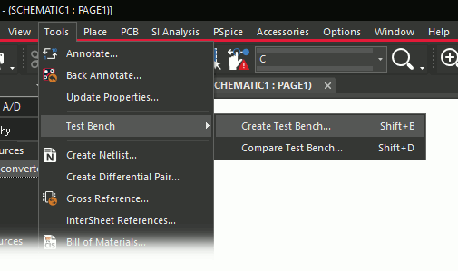
Step 3: Select Tools > Test Bench > Create Test Bench from the menu to create a new test bench.
Step 4: Enter Boost_Converter_Simplified for the Test Bench name and click OK to create the test bench.
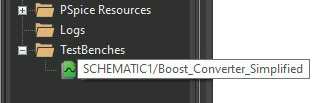
Step 5: A new TestBenches folder is shown in the Project Manager. Double-click the enclosed file to open the test bench.
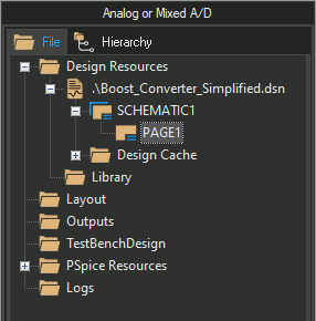
Step 6: The Project Manager for the test bench opens. Expand Boost_Converter_Simplified.dsn > SCHEMATIC1 and double-click PAGE1 to open the test bench page.
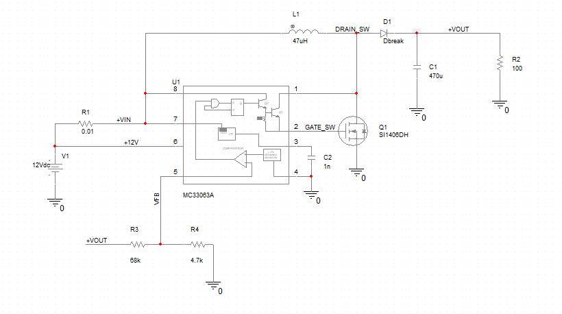
Step 7: View the schematic. The schematic canvas opens to a grayed-out view of the provided schematic. All symbols are disabled by default. To run a sectional simulation, the relevant components must be enabled.
Enabling Test Bench Components
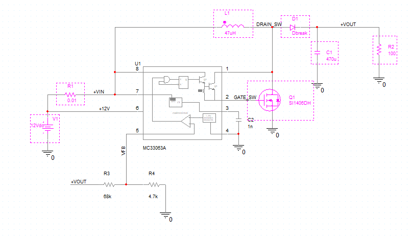
Step 8: Hold CTRL on the keyboard and click to select V1, R1, L1, D1, C1, R2, and Q1.
Step 9: Right-click any of the selected parts and select TestBench > Add Part(s) to Self.
Note: If the TestBench option is not available, perform steps 8 and 9 in the original schematic. Return to the test bench.
Step 10: Click anywhere in the schematic canvas to deselect the components. View the schematic. The components are now in their original colors.
Finding and Correcting Floating Nets
Note: Floating nets will produce errors during the simulation. This section will teach you how to identify and resolve floating nets.
Step 11: Select Edit > Find from the menu.
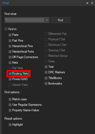
Step 12: The Find panel opens. Uncheck all entries under Find In and check Floating Nets.
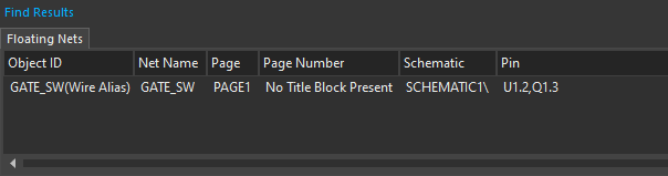
Step 13: Select Find. All floating nets are listed in the Find Results tab at the bottom of the window. Net GATE_SW is unconnected. This net can be connected to a voltage source to prevent the error.
Step 14: Select Place > PSpice Part > Source > Voltage Sources > Pulse from the menu.
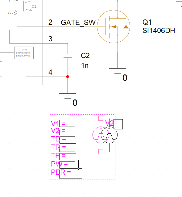
Step 15: Click to place the source in the schematic just under Q1. Right-click and select End Mode.
Step 16: Double-click the V1 parameter to change it.
Step 17: Enter 12V for the value and click OK.
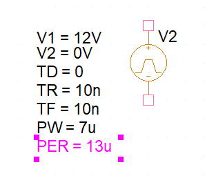
Step 18: Repeat this process to change the following values:
- V2: 0V
- TD: 0
- TR: 10n
- TF: 10n
- PW: 7u
- PER: 13u
Step 19: Select Place > Wire from the menu, the Wire button on the toolbar, or press W on the keyboard.
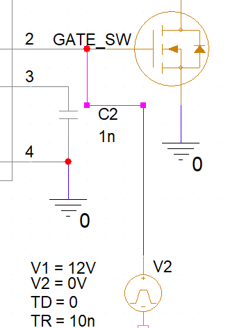
Step 20: Click to draw a wire between the source positive and net GATE_SW. Press Escape on the keyboard when finished.
Step 21: Select Place > PSpice Part > PSpice Ground from the menu.
Step 22: Click to place the ground at the bottom of V2. Right-click and select End Mode when finished.
The partial schematic is wired and can be simulated.
Creating a Simulation Profile
Step 23: To create a simulation profile for the section, select PSpice > New Simulation Profile from the menu.
Step 24: Enter BOOST_SECTION for the name and click Create.
Note: If the Simulation Manager Product Choices window opens, select the appropriate license and click OK.
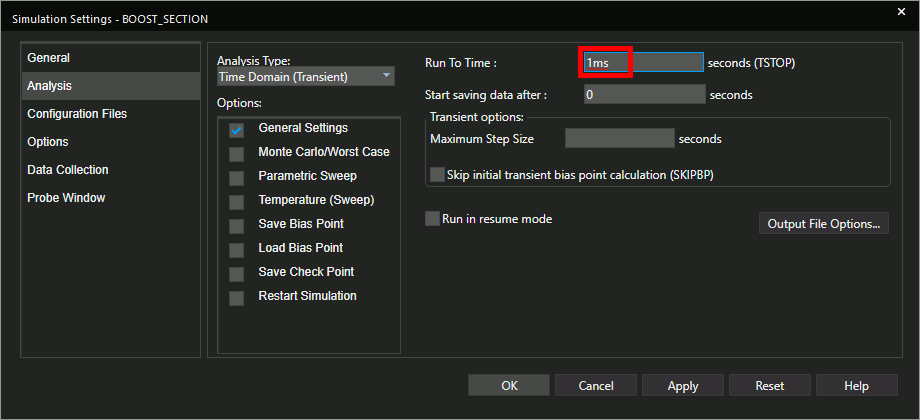
Step 25: Set the Run To Time to 1ms in the Simulation Settings window. Leave the other settings as the defaults and click OK.
Step 26: Select the Voltage/Level Marker button from the toolbar.
Step 27: Click to place probes on the +VOUT and GATE_SW nets. Right-click and select End Mode when finished.
Simulate Sections of Your Schematic
Step 28: Select PSpice > Run from the menu to start the simulation.
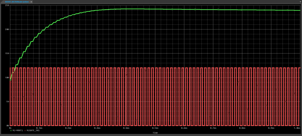
Step 29: View the simulation results. The boost converter topology runs without U1.
Wrap Up & Next Steps
Quickly simulate sections of your schematic designs to quickly analyze critical aspects of large, complex designs with test benches in PSpice. Test out this feature and more with a free trial of OrCAD.
Want to learn more about PSpice? View additional how-tos, walk-throughs, and courses at EMA Academy.

