With the schematic completed, layout file created, and outline drawn, the next step in the design process is to place components on the board. Components are often placed according to schematic connectivity to keep connections short, and many components have specific requirements for placement, such as smoothing capacitors. An efficient method to identify and place critical components in the PCB design is to cross-probe and cross-place between the schematic and PCB. OrCAD Capture and OrCAD PCB Designer include bi-directional communication, allowing you to seamlessly place components on the PCB from the schematic with cross-placement.
This quick how-to will provide step-by-step instructions on how to place components on the PCB from the schematic with cross-placement in OrCAD.
To follow along, download the provided files above the table of contents.
How-To Video
 Open in New Window
Configuring the Design for Cross-Placement
Step 1: Open the provided design in OrCAD Capture.
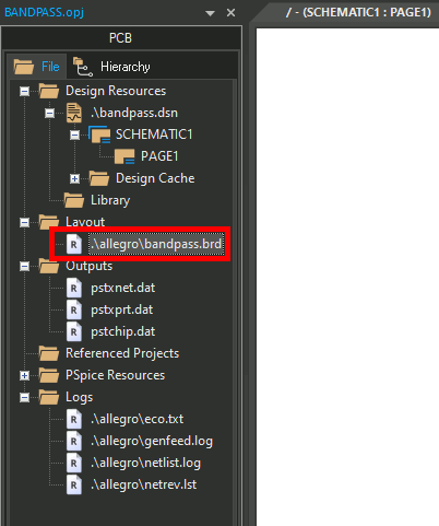
Step 2: Double-click the layout in the Project Manager to open OrCAD PCB Designer.
Step 3: Move the windows for Capture and PCB Designer to create a split-screen configuration.
Note: If your system has multiple monitors, you can put Capture in one monitor and PCB Designer in another to improve visibility.
Step 4: In Capture, select Options > Preferences from the menu.
Step 5: The Preferences window opens. Select the Miscellaneous tab.
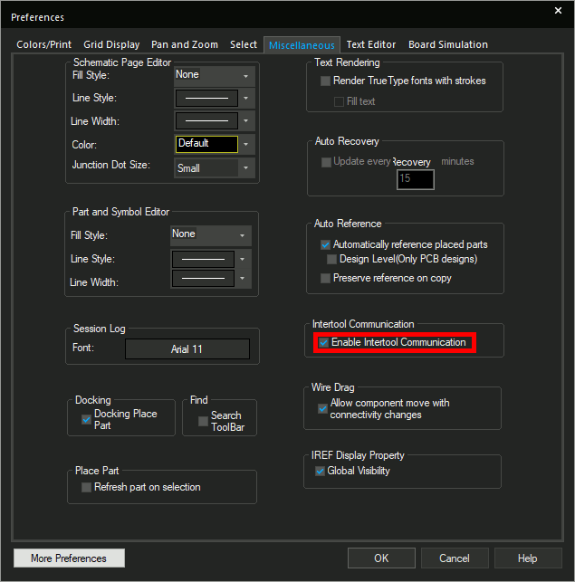
Step 6: Check the option for Enable Intertool Communication. Click OK.
Note: This will allow for parts selected in Capture to automatically be selected in PCB Designer.
Place Components on the PCB from the Schematic
Step 7: Select Place > Components Manually from the PCB Designer menu. The Placement window opens.
Step 8: Click Hide to minimize the window but leave it active.
Note: Do not click Close to close the window. Components cannot be placed if the window is closed.
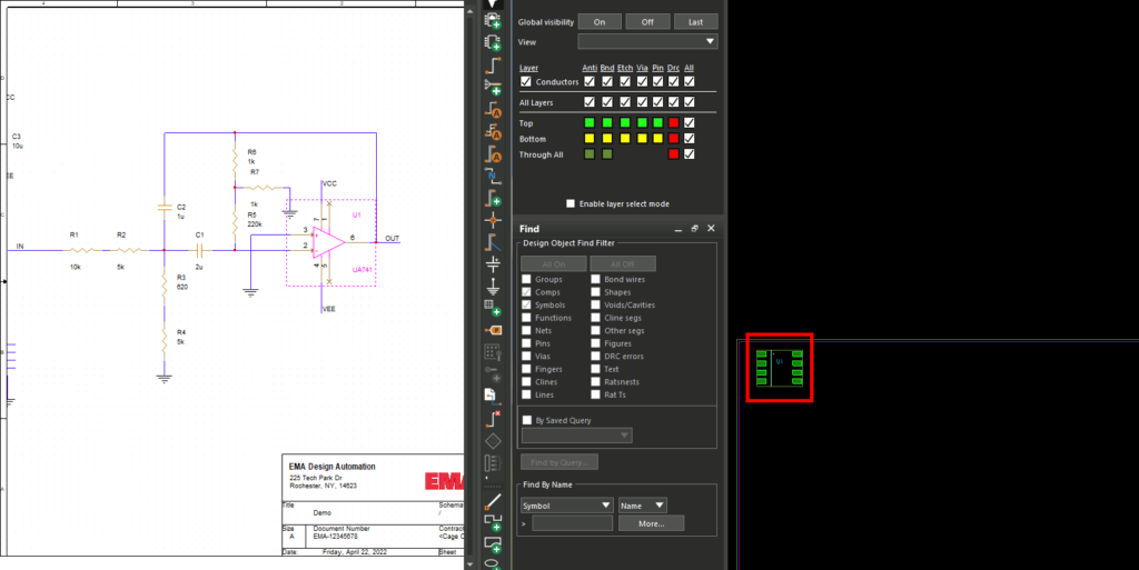
Step 9: Select a part in Capture. The footprint is attached to the cursor in PCB Designer.
Step 10: Click to place the part in the PCB canvas.
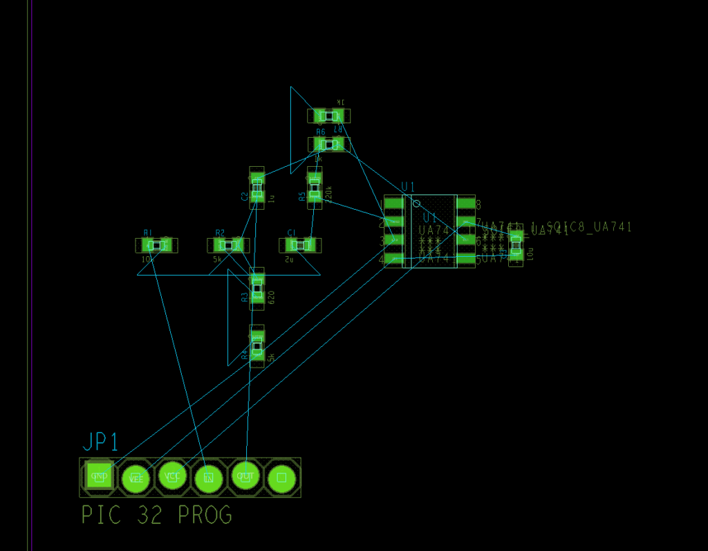
Step 11: Select the remaining footprints in Capture and click to place in PCB Designer. When finished, right-click and select Done.
Wrap Up & Next Steps
Quickly place components on the PCB from the schematic with cross-probe and cross-placement features in OrCAD. Test out this feature and more with a free trial of OrCAD.
Want to learn more about Capture and PCB Designer? Get access to free how-tos, courses, and walk-throughs at EMA Academy.

