Signal integrity (SI) and power integrity (PI) analysis is crucial to verify performance of high-speed and complex designs before production. When using different ECAD tools for PCB layout and simulation, it can be difficult to translate designs with the required level of accuracy and information to perform a realistic simulation. Sigrity allows you to translate PCBs, extract topologies, and perform SI/PI analysis on Altium Designer projects to:
- Efficiently analyze signal integrity and power integrity
- Verify and improve design performance
- Perform post-layout exploration and optimization
- Simulate and verify compliance to industry standards
- Signoff on your PCB design with confidence
This quick how-to will provide step-by-step instructions on how to export a design in Altium Designer version 2021 or higher and bring the design (ODB++) into Sigrity for signal integrity and power integrity analysis.
Configuring an Altium Design for Export
Step 1: Load your Altium PCB project in Altium Designer 2021 or above.
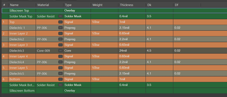
Step 2: Launch the Layer Stack Manager and confirm the stackup is configured correctly including:
- Layer thicknesses
- Copper weights
- Dieletric Constant (Dk)
Note: The material’s dielectric constant must be entered accurately per the manufacturer specifications for the stackup material included in the design.

Step 3: Add an ODB++ section to your OutJob. This will be specifically configured for the output to Sigrity.
Note: Using an OutJob will streamline the process of exporting your updates or physical changes you are making in Altium into Sigrity through an ODB++ workflow. If you are not used to using an OutJob in Altium, get instructions here.
Step 4: Right-click on the ODB++ section of the OutJob to configure the settings.
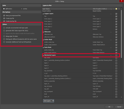
Step 5: Uncheck Mechanical Layers so you just have the important electrical layers of the PCB in the ODB++ export.
Step 6: Uncheck all the options under Others.
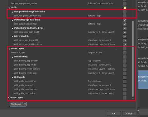
Step 7: Scroll down in the configuration window. Uncheck the following under the Drills category:
- All non-plated holes
- Any drills that are not needed for conductivity
- Any drill that may not be connected to the electrical nets of the design
Step 8: Uncheck Other Layers to turn off the Drill drawing and Drill guide layers.
Note: If these layers are selected when you import, drill drawing symbols will be included which may hinder your ability to work with the board in Sigrity.
Step 9: Select OK to save the ODB++ configuration.
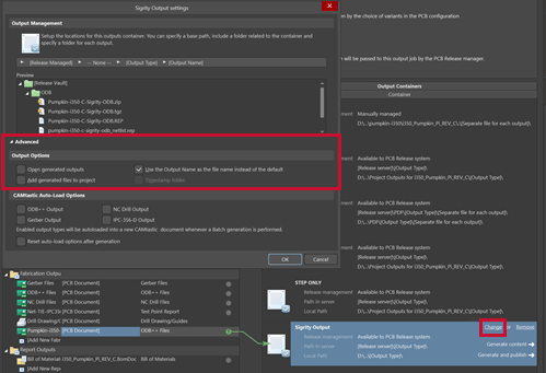
Step 10: With the Sigrity Output still selected, click Change to configure the output container.
Step 11: Change the output options so that you have a separate output container and can easily find your result.
Step 12: Deselect the following options in the Advanced Output Options:
- Open Generated Outputs
- Add Generated Files to Project
Step 13: Select to Use the Output Name as the file name instead of the default.
Step 14: Click OK to save the Output Settings.
Step 15: Run the OutJob and generate the ODB++ output.
Step 16: Locate the Sigrity_ODB.tgz file. Copy the Sigrity_ODB.tgz file and paste it in another location on your computer. This should be the location of the actual simulation project you will be working on moving forward.
Importing an Altium Designer Project into Sigrity
Step 17: Launch Sigrity Topology Workbench version 2022 or above and click on New Project.
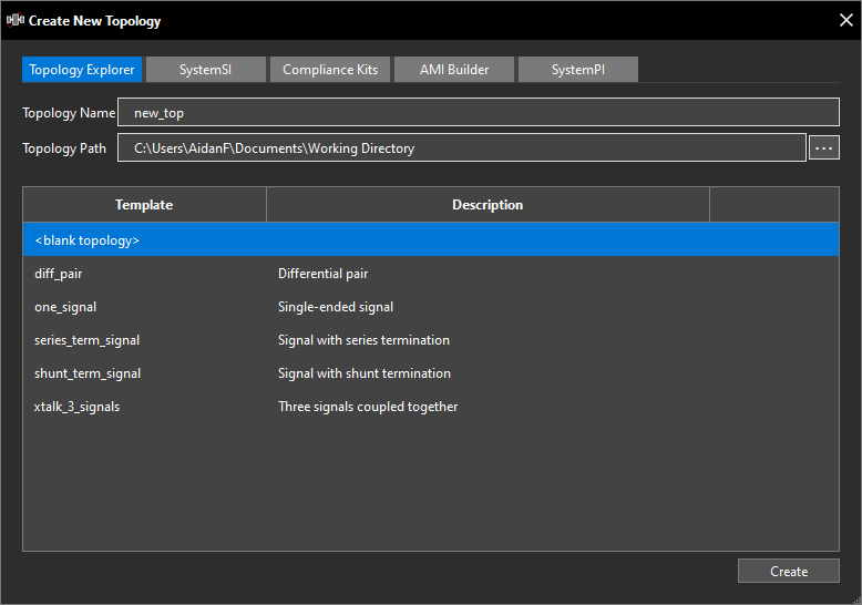
Step 18: Ensure Blank Topology is selected. Under Topology Name, enter a name for the topology that is consistent with what you will be simulating.
Step 19: Under Topology Path, browse to the directory location with the Sigrity_ODB.tgz file and click Open.
Step 20: Click Create.
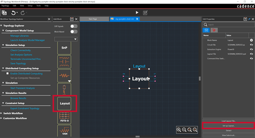
Step 21: Drag and drop a Layout block onto the topology.
Step 22: Double-click the layout block to edit the block properties. By default, the block is preloaded with a sample SPD layout file for a SODIMM which we will override.
Step 23: Change the Extraction Engine to Power SI.
Step 24: Select Set up Layout to launch Layout Workbench.
Configuring Translator Settings in Sigrity
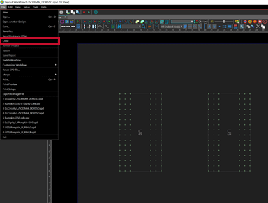
Step 25: In Layout Workbench, select File > Close to close the sample SODIMM file that was opened by default.
Step 26: Select Tools > Options > Edit from the menu.
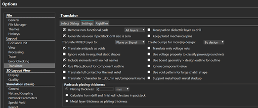
Step 27: Under Layout, select Translator. Configure the options as seen above then click OK.
Note: These options are saved within Sigrity. Once these settings are configured, they will be automatically applied to future projects and translations.
Importing an Altium Designer Project into Sigrity
Step 28: In the Layout Setup section of the Model Extraction Workflow, select Load Layout File.
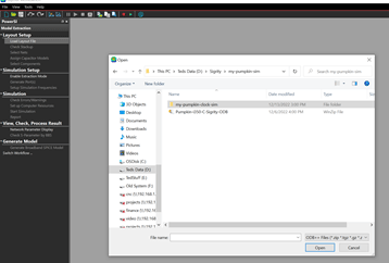
Step 29: Browse to the location of the Sigrity_ODB.tgz file. Select the file and click Open.
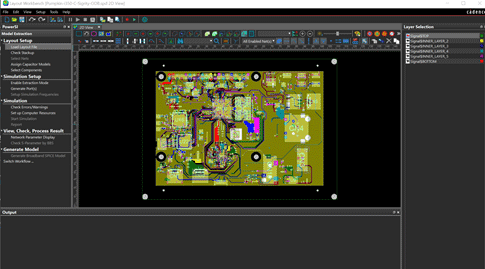
Step 30: View the imported Altium design in Sigrity.
Step 31: Under Layout Setup, select Check Stackup. View the stackup and verify that the information translated correctly including the layer thickness and material properties such as the Dielectric Constants.
Note: This information may be incorrect if you are not using Altium 21 or above. Fill in any missing or incorrect information manually in the stackup table.
Extracting a Topology from an Altium Designer Project for SI/PI Analysis
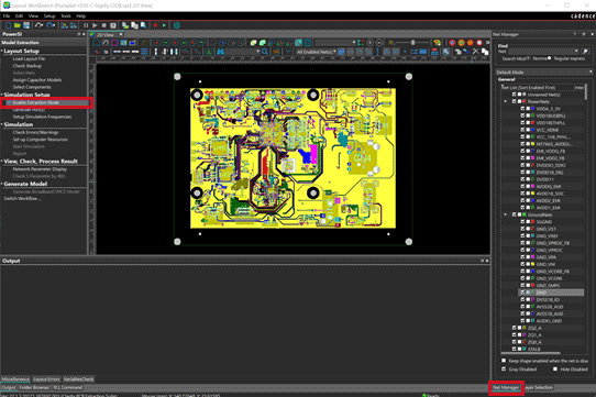
Step 32: Under Simulation Setup, select Enable Extraction Mode.
Step 33: In the bottom right corner of the Sigrity Layout Workbench canvas, select Net Manager.
Step 34: In the Net Manager, right-click on the main ground net in the design and select Split Open Nets.
Step 35: A dialog box should display stating there are No Open Nets Detected. Click OK.
Note: This step is performed to verify the design was translated correctly. If the ground net is turned into open nets, the vias were not configured correctly when you exported the ODB++ file in Altium and Sigrity is seeing all the ground pours as being separated. Return to Altium and reconfigure the settings for the ODB++ export.
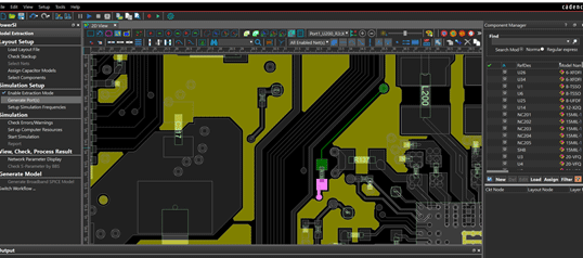
Step 36: Under Layout Setup, choose Select Nets. Select the nets you want to analyze.
Step 37: Under Simulation Settings, select Generate Ports. Follow the wizard to setup the ports.
Step 38: Under Simulation Setup, select Setup Simulation Frequencies. Configure the frequencies for the simulation.
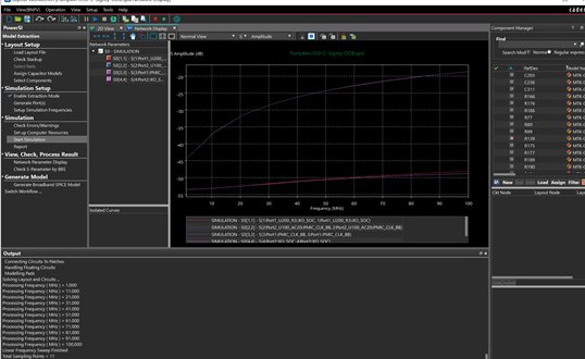
Step 39: Select Start Simulation. When the simulation is complete, results will be generated containing both an S-Parameter file and an SPD file that can be linked within Topology Workbench and used to perform full system-level simulation.
Step 40: Save and close the Layout Workbench project.
Perform SI/PI Analysis on Altium Designer Projects in Sigrity
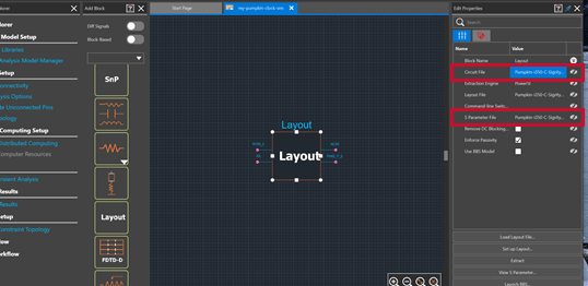
Step 41: Back in Topology Explorer with the Layout block still selected, select the Circuit File. This should be configured as the SPD file that was generated in Layout Workbench.
Step 42: Confirm the S-Parameter file is now configured as the S-Parameter file generated from the Layout Workbench extraction.
Step 43: Continue with simulation and analysis in Topology Explorer using the extracted traces from your Altium design.
Note: If you make changes in Altium to your layout, rerun the OutJob and replace the ODB++ file within Topology Explorer by selecting Load Layout File. Then select Extract to regenerate the SPD and S-Parameter file and automatically link the files in Topology Explorer.
Wrap Up & Next Steps
Easily translate and extract Altium PCBs to perform SI/PI analysis on Altium Designer projects using Sigrity to evaluate signal integrity, power integrity, and PCB performance. Get more step-by-step instructions for Sigrity at EMA Academy.