With the increasing speeds and frequencies of today’s electronic designs, any interference between different signals can degrade performance, causing issues including signal distortion, timing errors, and loss of data integrity. Performing coupling analysis early in the design process can help to identify unwanted electromagnetic interference (EMI) and crosstalk between signals on a PCB allowing designers to mitigate issues during the design process and ensure reliable signal transmission. Coupling analysis in OrCAD X Presto provides an efficient method to analyze coupling directly in the PCB canvas with:
- Easy to configure simulations
- Color-coded visual overlays
- Tabular results
- Cross-probing between simulation results and the PCB canvas
- Unified environment for design and analysis
This quick how-to will provide step-by-step instructions on how to perform coupling analysis in OrCAD X Presto.
To follow along, download the provided files above the table of contents.
How-To Video
 Open in New Window
Activating Coupling Analysis in OrCAD X Presto
Note: A separate installation is required to perform impedance analysis and coupling analysis. For help configuring the installation and more information view the how-to here.
Step 1: Open the provided design in OrCAD X Presto.
Step 2: Select View > Panels > Analysis Workflows from the menu.
Step 3: In the Analysis panel, ensure the drop-down selection is configured as Coupling Analysis.
Performing Coupling Analysis in OrCAD X Presto
Step 4: Under Analysis Modes, select Net Based.
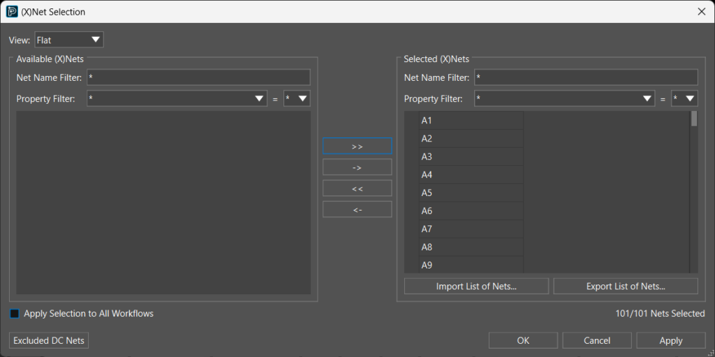
Step 5: Choose Select Nets.

Step 6: Click >> to select all the nets in the design for analysis then click OK.
Note: For more information on performing coupling analysis, view our free workshop here.
Step 7: Select Start Analysis. A progress bar displays the status of the simulation. When the analysis is complete a green check mark will appear next to Start Analysis.
Evaluating Coupling Analysis Results in OrCAD X Presto
Step 8: Under View Modes, ensure Net Based and Worst Case are selected.
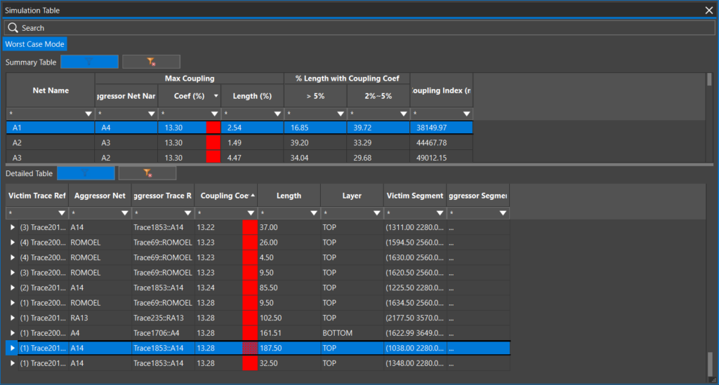
Step 9: Select View Coupling Tables. This provides tabular results including a summary of the coupling for nets in the design and detailed information. Coupling results are reported using a color-coded scale with blue being a low coupling coefficient and red being a high coupling coefficient.
Step 10: Select the Max Coupling Coef (%) twice to filter the column to view the traces with the highest coupling coefficient.

Step 11: Select A1 in the Summary table and click the Coupling Coefficient column in the detailed table to sort the results.
Step 12: Double click the line item for Victim Trace2011::A1, Aggressor trace A14, and length 187.5 to be brought to the location on the PCB canvas.
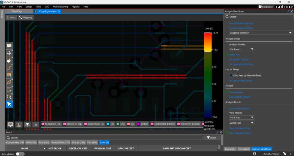
Step 13: In the Analysis panel, select View Coupling Visions.
Step 14: Slide the coupling bar up to filter the coupling vision to only high coupling nets.

Step 15: View the result. There are several traces in red identifying high coupling coefficients that can be resolved be increasing the spacing between the critical nets.
Correcting Coupling Issues in Your PCB Design
Step 16: Select View Coupling Visions again to turn off the coupling view in the PCB canvas.

Step 17: Select Slide from the toolbar.
Step 18: In the options, select Assisted and choose to Shove traces.
Step 19: Select trace A1 and slide it up slightly further away from the aggressor net, A14, to resolve the error.
Note: Tab can be used to filter through the objects on the PCB canvas for efficient selection. For more granularity in the placement of traces and components, smaller grid values can be configured by selection Grids in the PCB canvas.
Step 20: Press Escape on the keyboard and choose the Select tool on the toolbar when finished.
Verifying the Effects of Design Modifications on Coupling
Step 21: In the Analysis Workflows panel, select Start Analysis.
Step 22: In the Save Analysis Results pop-up, select Ignore.
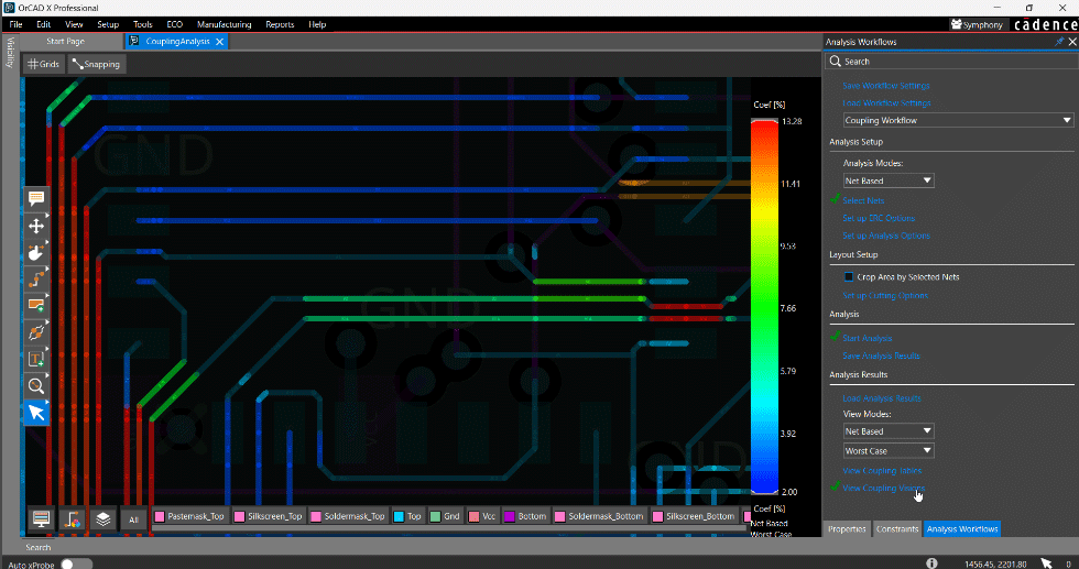
Step 23: When the analysis is complete, select View Coupling Visions.

Step 24: View the results. Moving the trace has decreased the coupling between nets. This process can be completed throughout the PCB design process to identify coupling and improve signal integrity.
Wrap Up & Next Steps
Mitigate unwanted coupling and improve signal integrity for your designs by performing coupling analysis in OrCAD X Presto throughout the PCB layout. Get more step-by-step instructions for OrCAD X at EMA Academy.
