After a schematic has been drawn and approved, the next step is to migrate the design from paper to board through the generation of a netlist and parts list detailing the components and connections. Easily netlist a design in OrCAD Capture with the generation of a netlist and parts list in a single step.
This quick how-to will provide step-by-step instructions on how to netlist a design in OrCAD Capture.
To follow along, download the provided files above the table of contents.
How-To Video
 Open in New Window
Checking PCB Footprints
Note: PCB footprints must be assigned to all components in the design for netlisting.
Step 1: Open the provided design in OrCAD Capture.
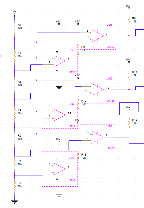
Step 2: Hold CTRL on the keyboard and select op-amps U1A-U1D and U2A-U2B.
Step 3: Right-click one of the selected components and select Edit Properties.
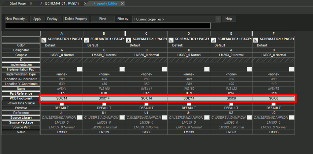
Step 4: The Property Editor window opens for all components in the design. Ensure that each component has a value assigned in the PCB Footprint row.
Note: If this value is blank for any components, those components need to have footprints assigned. Learn more about how to assign footprints here.
Step 5: In this case, all components have PCB footprints assigned and the netlist can be created. Close the Property Editor tab.
Netlist a Design in OrCAD Capture
Note: Generating only a netlist is ideal when outsourcing the PCB layout to another team of CM.
Step 6: Select Tools > Create Netlist from the menu.
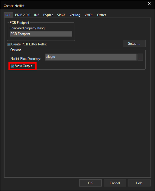
Step 7: The Create Netlist window opens. Check View Output to view the generated netlist files in Capture.
Step 8: Enter allegro into the Netlist Files Directory field.
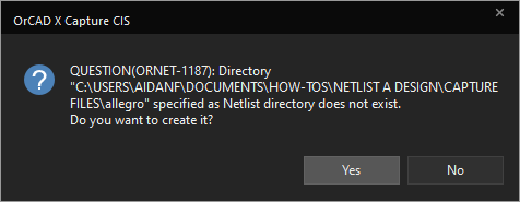
Step 9: Click OK. A prompt appears that the allegro folder must be created before the files can be generated. Click Yes to create the folder.
Step 10: The tabs for pstxprt.dat, pstxnet.dat, and pstchip.dat open in the Capture window. View and close the tabs.
Note: These files contain the following information:
- pstxprt.dat: Part names and sections
- pstxnet.dat: Node and net data
- pstchip.dat: Matches the library parts with their primitive models.
Netlist a Design in OrCAD Capture and Create a PCB Layout
Note: A netlist and PCB layout can be created in a single step to accelerate the process PCB design process. This links the schematic and PCB together and creates an efficient method to communicate changes between OrCAD Capture and OrCAD PCB Designer.
Step 11: Select PCB > New Layout from the menu.
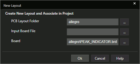
Step 12: The New Layout window opens. Leave the default settings and click OK.
Note: From this window, you can specify the PCB layout folder, board file name, and input board file if generating a layout from an existing board file.
Step 13: The Product Choices window opens for PCB Designer. Select the appropriate license and click OK.
Step 14: OrCAD PCB Designer opens automatically and has already imported the required files to communicate schematic connectivity. To verify component sync, select Place > Components Manually from the PCB Designer menu.
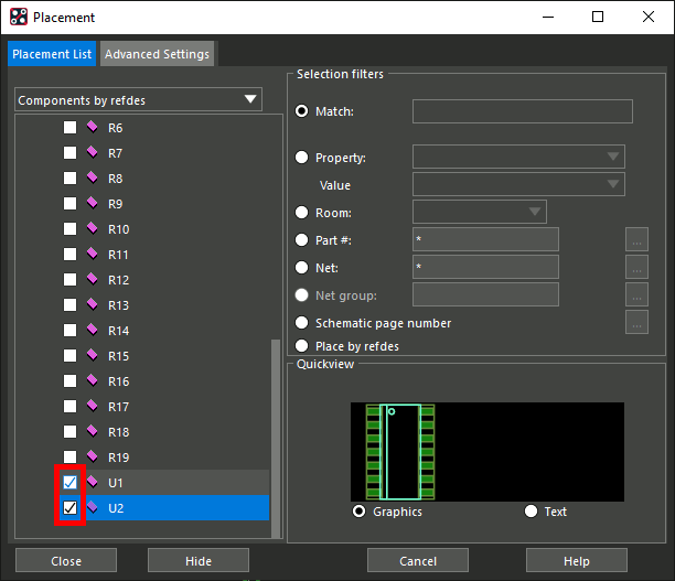
Step 15: The Placement window opens. Check the options for U1 and U2 to place them in the canvas.
Step 16: Click Hide to hide the placement window to make the canvas easier to see.
Note: Do not close the Placement window. This will cancel the placement command.
Step 17: Click to place the components. Right-click and select Done when finished.
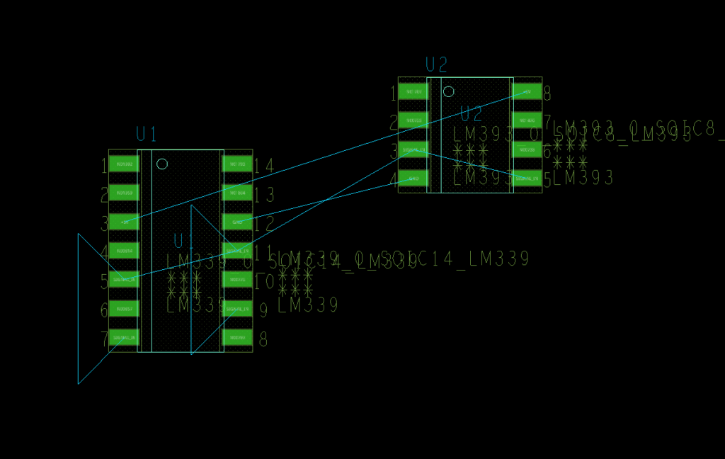
Step 18: View the canvas. Ratsnest lines show the required connections between pins, indicating that nets and pin assignments were imported successfully.
Wrap Up & Next Steps
Quickly netlist a design in OrCAD Capture to communicate the schematic design, components, and connections for PCB layout. Test out this feature and more with a free trial of OrCAD. Want to learn more about Capture? Get access to free how-tos, courses, and walk-throughs at EMA Academy.

