While many designers picture PCB design as a two-dimensional task, with increasing mechanical restrictions, failing to take component height and placement into account may lead to costly respins and redesigns towards the end of the design process. OrCAD X Presto allows you to efficiently map a 3D model to components to visualize the PCB assembly in 3D and identify any potential errors or collisions before production.
This quick how-to will provide step-by-step instructions on how to map a 3D model to components with the Footprint Editor in OrCAD X Presto.
Using OrCAD X PCB Designer? Learn how to work with 3D models here.
To follow along, download the provided files above the table of contents.
How-To Video
 Open in New Window
Activating the Footprint Editor in OrCAD X Presto
Note: In OrCAD X Presto, 3D models for components must be mapped to component footprints in the Footprint Editor.
Step 1: Open OrCAD X Presto. Select Open in the Start page.
Step 2: Browse to the included Footprints folder and select the 1x06_lock.dra file. Click Open to open the file.
Map a 3D Model to Components
Step 3: In the Properties panel, under Status, select the plus sign for 3D Model to add a 3D model. The view switches to a 3D rendering of the footprint.
Step 4: Browse to the provided 3D Models folder and select Conn1x6 from the provided materials. Click Open.
Step 5: View the 3D canvas. The 3D model is added and is automatically mapped correctly with the footprint.
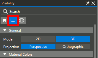
Step 6: Open the Visibility panel and select the Display mode.
Step 7: Select 2D under General to change the view to 2D to save.
Step 8: Select File > Save from the menu. Click Yes when prompted to overwrite.
Map a 3D Model to Components: Manual Adjustment
Note: The mapping of some 3D models may need to be completed manually to achieve the correct position and orientation.
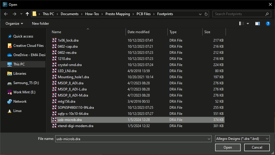
Step 9: Select File > Open from the menu. Select the provided usb-microb.dra file and click Open.
Step 10: Select the plus sign for 3D Model in the Properties panel.
Step 11: Browse to the provided 3D Models folder and select USB_MicroAB.STEP. Click Open.
Step 12: View the 3D canvas. The USB connector has been mapped but is off-center.
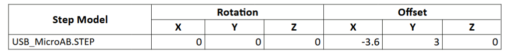
Step 13: Scroll to 3D Location in the Properties panel. Mapping can be performed with the following options:
- Manual: Click-and-drag manual adjustment in the X, Y, and Z directions
- Top: Snapping the model to the top of the footprint
- Bottom: Snapping the model to the bottom of the footprint
- XY, Z: Snapping 3D features to pads or footprint features
- Offset and Rotation: Adjusting the X, Y, and Z coordinates numerically
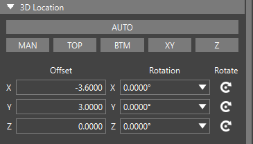
Step 14: Define the following STEP mapping parameters for the USB connector:
Map a 3D Model to Components: Snapping
Step 15: Select Z under 3D Location.
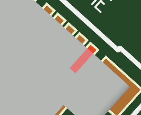
Step 16: Select one of the pads on the connector footprint. The pad is highlighted in red.
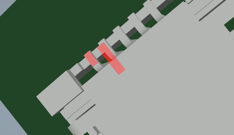
Step 17: Pan to the bottom of the connector and select the corresponding pin. The pin is highlighted in red as well.
Note: Hold Shift and click and drag the middle mouse button to pan the view.
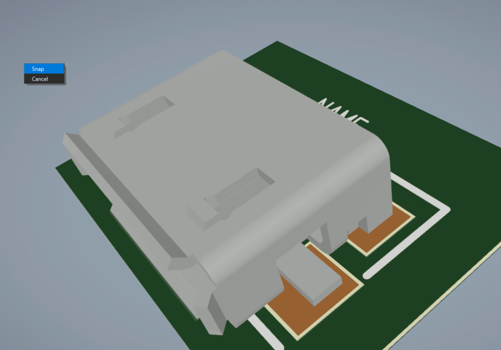
Step 18: Right-click and select Snap. The USB connector and footprint are aligned in the Z direction automatically.
Step 19: Open the Visibility panel and select the Display mode.
Step 20: Select 2D under Mode.
Step 21: Select File > Save from the menu. Click Yes if prompted to overwrite.
Confirm the Footprint and 3D Model Mapping
Step 22: Open the provided presto_tutorial.brd file in Presto.
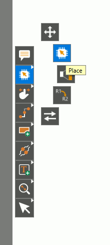
Step 23: Right-click the Move mode in the toolbar and select the Place mode.
Step 24: Select the Unplaced Components hyperlink in the Properties panel. The Search panel opens to show the two components mapped earlier, which are unplaced.
Step 25: Select JP2 from the list to attach the part to your cursor.
Step 26: Click to place JP2 in the PCB canvas.
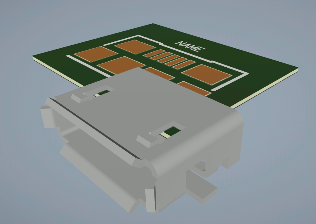
Step 27: Select the Unplaced Components hyperlink and click X1 to place the USB connector.
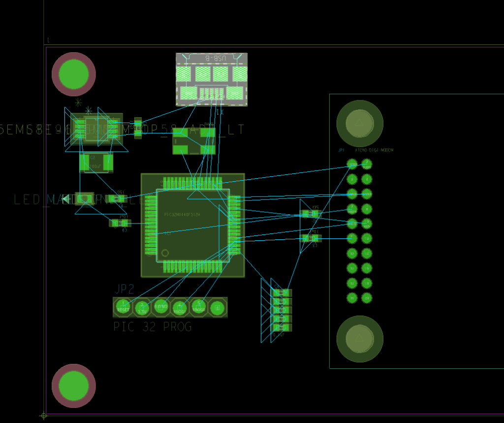
Step 28: Press R on the keyboard twice to rotate the connector 180° and click to place the connector.
Step 29: Press Escape on the keyboard to return to the Select mode.
Step 30: Open the Visibility panel and select the Display mode.
Step 31: Select 3D under Mode.
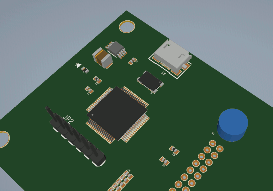
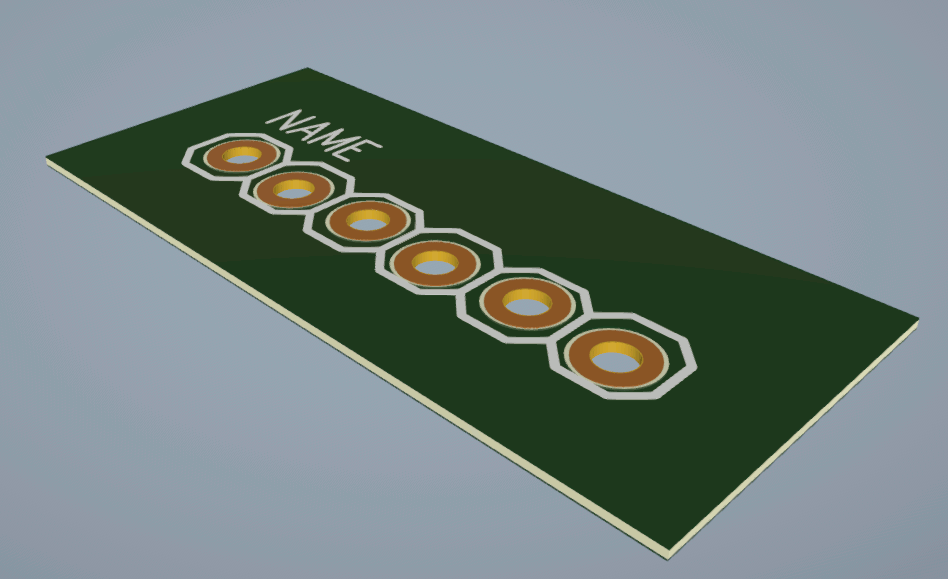
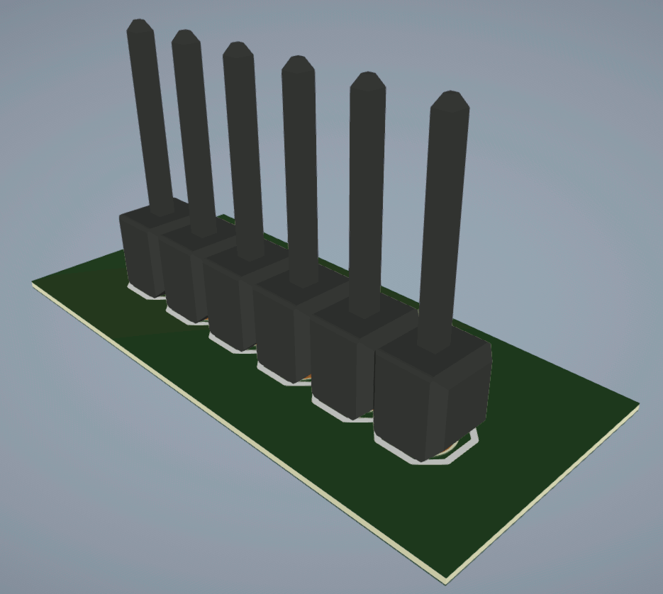
Step 32: View the 3D render of the board. The 6-position header and USB connector have been added.
Step 33: Select 2D to return to the 2D canvas.
Wrap Up & Next Steps
Quickly assign and map a 3D model to components to verify the final PCB assembly and achieve first-pass design success with OrCAD X Presto. Don’t have OrCAD X Presto? Get your free trial here and for more step-by step instructions and walk-throughs on using OrCAD X Presto visit EMA Academy.
