Many components in your design will require a specific footprint defined by the manufacturer; however, some components will likely use standardized footprints such as SOIC or DIP. Included PCB Footprint Libraries in OrCAD PCB Designer contain commonly used footprints to help you jump start the design creation process.
This quick how-to will provide step-by-step instructions on how to find and browse available PCB footprint libraries in OrCAD PCB Designer.
How-To Video
 Open in New Window
Locating Included PCB Footprint Libraries in File Explorer
Step 1: Open File Explorer to the main C:\ drive.
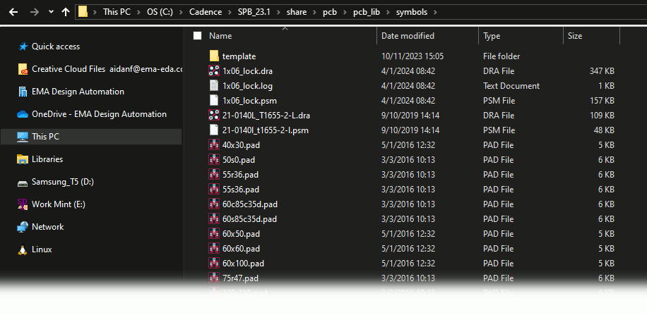
Step 2: Navigate to C:\Cadence\SPB_[version]\share\pcb\pcb_lib\symbols by browsing through the files. All included PCB footprint libraries for OrCAD are stored here.
Viewing and Browsing PCB Footprint Libraries in OrCAD
Note: The following method can be used to find available PCB footprints for schematic symbols in OrCAD Capture.
Step 3: Open OrCAD PCB Designer.
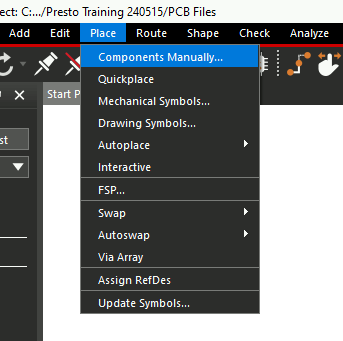
Step 4: Select Place > Components Manually. The Placement window opens.
Note: If a design is opened in OrCAD PCB Designer, this window is populated with the components to place.
Step 5: Select the Advanced Settings tab at the top of the window.
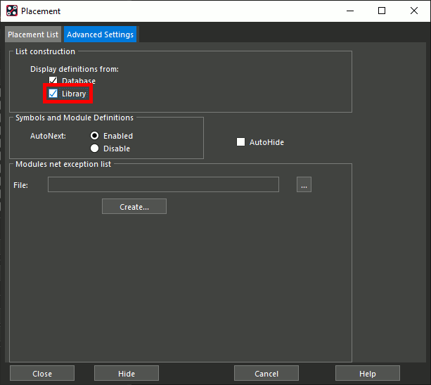
Step 6: Check Library under Display Definitions From.
Step 7: Return to the Placement List tab.
Step 8: Select Package Symbols from the dropdown at the top of the window. The window is populated with a list of all available package symbols.
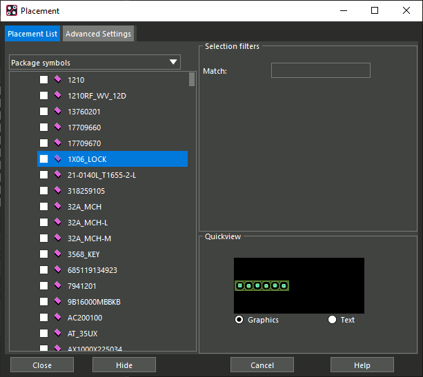
Step 9: Select an entry in the list. A preview of the footprint is shown.
Searching for Footprints by Name
Step 10: To find a footprint by name, enter the desired name into the Match text field under Selection Filters and press Enter. In this example, we will enter LED_LNJ.
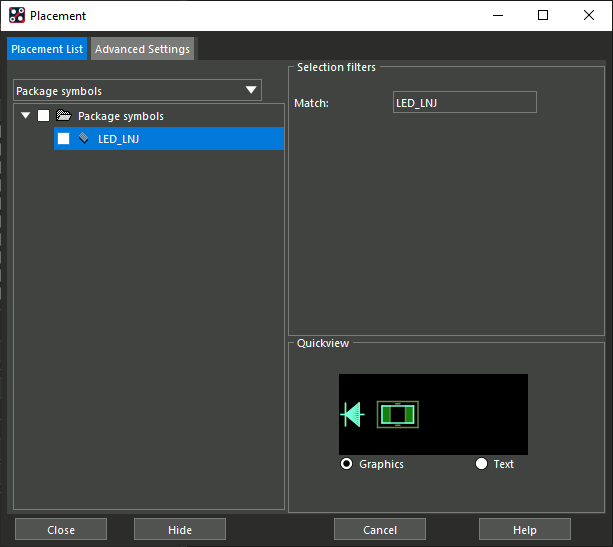
Step 11: View the result list. The single entry LED_LNJ is shown.
Note: OrCAD will only list footprints whose names exactly match what is typed into the search field. Wildcard characters can be used to find less specific footprints. The asterisk can be used to indicate any combination of unknown characters.
Step 12: Enter *0402* into the search field and press Enter.
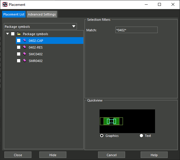
Step 13: View the result list. All components with the string “0402” somewhere in the name are listed.
Step 14: Enter SM?0402 into the search field and press Enter.
Note: The question mark indicates a single unknown character.
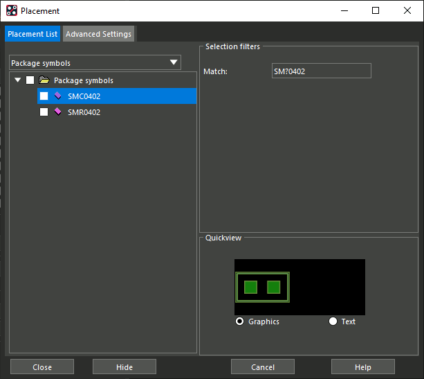
Step 15: View the result list. Any components whose names start with SM and end with 0402 with a single character in-between are listed. In this case, two results are listed; SMC0402 and SMR0402.
Wrap Up & Next Steps
Quickly find and use common footprints in your design with the included PCB footprint libraries in OrCAD PCB Designer. Test this feature and more with a free trial of OrCAD. Get more how-tos for OrCAD at EMA Academy.
Looking for additional libraries containing pre-built and verified schematic symbols, PCB footprints, and 3D Models? Check out the Unified Search feature.

