With today’s designs becoming more compact, ensuring that all components fit on the board and into the mechanical housing is a crucial step in the design process. While designing a board based on the enclosure will help, a 3D view as well as checking for clearances and collisions are the most effective way to ensure fitment in all dimensions and avoid costly respins. OrCAD X Presto includes the ability to quickly check and correct 3D clearance errors (3D DRC errors) directly from the PCB canvas and 3D canvas.
This quick how-to will provide step-by-step instructions on how to find and correct 3D DRC errors in OrCAD X Presto.
To follow along, download the provided files above the table of contents.
How-To Video
 Open in New Window
Defining 3D DRC Constraints
Step 1: Open the provided design in OrCAD X Presto.
Step 2: Select Tools > Constraint Manager from the menu.
Step 3: The Constraint Manager window opens. Select the 3D domain from the Worksheet Selector.
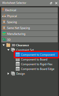
Step 4: Expand 3D Clearance > Constraint Set and select the Component to Component worksheet. The Component to Component constraint table opens.
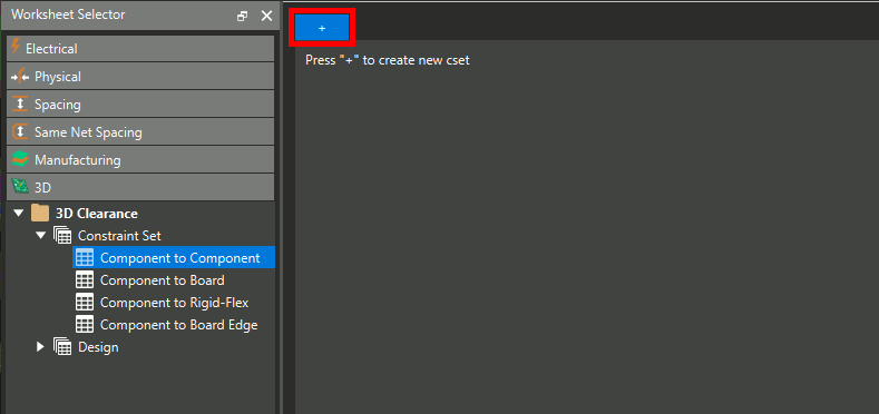
Step 5: Select the plus sign to create a new constraint set.
Step 6: The Create 3D CSet window opens. Enter PKG2PKG for the name, set the CSet Usage to Spacing3D, and click OK to create a new CSet.
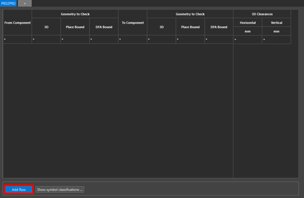
Step 7: The worksheet is populated with an empty table where component-to-component spacing values can be defined. To add a value for a specific component or group of components, select Add Row at the bottom of the table.
Step 8: The Create Clearances window opens. Select 1X06_LOCK in the From Component table.
Step 9: Click and drag in the To Component table or use CTRL+A on the keyboard to select all the components.
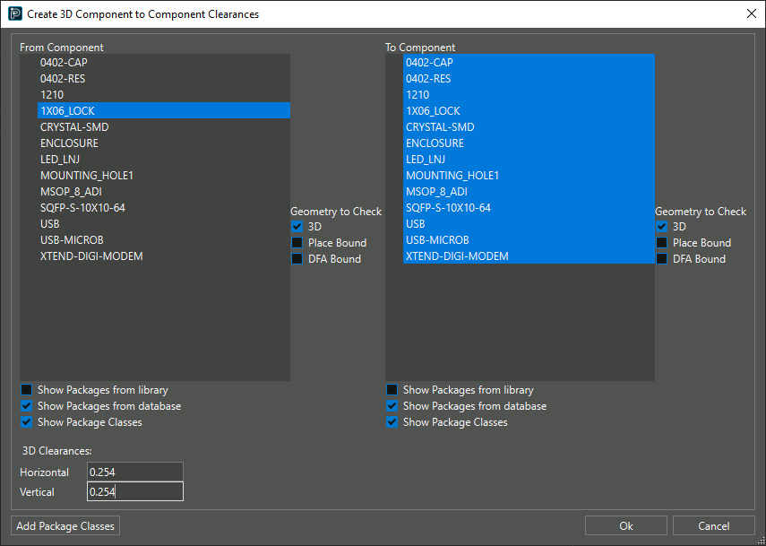
Step 10: Enter 0.254 for the Horizontal and Vertical 3D Clearances.
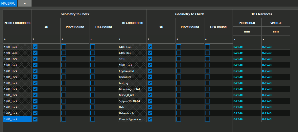
Step 11: Click OK. The relationships and constraints are automatically created and added to the table in the Component to Component worksheet.
Assigning 3D Constraints
Step 12: With the 3D constraint set defined, it must be assigned to the board before it can be checked. Select the 3D Clearance > Design > Component to Component worksheet.
Step 13: Select the cell under Referenced Package to Package 3D CSet for 3DDRC_Tutorial.
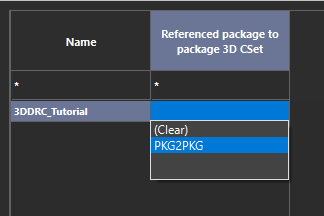
Step 14: A drop-down menu opens. Select PKG2PKG from the menu to assign the constraint set.
Activating 3D DRC Checks
Step 15: With constraints defined and assigned, constraint analysis must be activated before any DRCs errors are reported. Select Analyze > Analysis Mode from the menu. The Analysis Modes window opens.
Step 16: Select 3 Dimensional > Components from the list on the left.
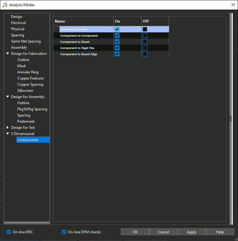
Step 17: From here, constraint checks can be enabled or disabled. Select the On checkbox for Mark All Constraints to activate all constraint checks.
Step 18: Click OK to save the settings and close the window. Close the Constraint Manager.
Checking for 3D DRC Errors
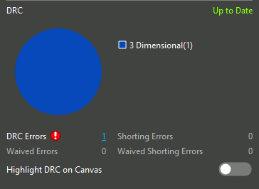
Step 19: View the Properties panel for the board. A pie chart is shown in the DRC subpanel, showing one 3D error in the design.
Note: If the DRC cache is listed as out of date, select Refresh to update it.
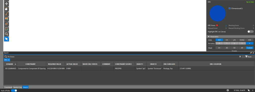
Step 20: Select the hyperlink for DRC Errors. The Search panel opens to show a list of errors in the design.
Step 21: Double-click the error to be brought to its location on the board.
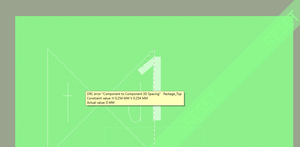
Step 22: Hover your cursor over the error for more information. This error reports a collision between the header JP2 and enclosure, as indicated by an actual spacing value of 0.
Viewing 3D DRC Errors in the 3D Canvas
Step 23: To fully visualize the 3D DRC errors, activate the 3D mode. To do this, select the Visibility tab on the side of the window.
Step 24: The Visibility panel opens. Select the Display mode.
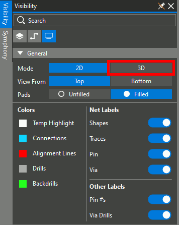
Step 25: Under General, select 3D for the Mode.
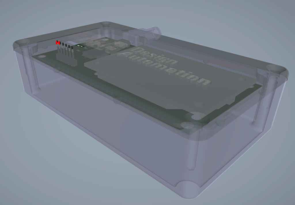
Step 26: The 3DX canvas opens with the same errors visible. Click and drag the middle mouse button to pan the view. Hold Shift on the keyboard and click and drag the middle mouse button to rotate the view.
Step 27: Select the hyperlink for DRC errors again to open the Search panel.
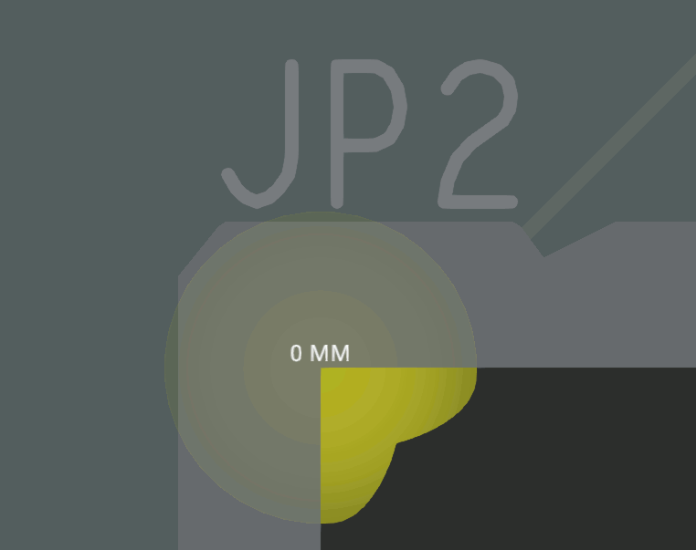
Step 28: Double-click the error between the enclosure and JP2. The view is panned to connector JP2, which quite obviously collides with the enclosure.
Correcting 3D DRC Errors in OrCAD X Presto
Step 29: Open the Visibility panel and select 2D to return to the 2D view mode.

Step 30: Select the Move mode from the toolbar.
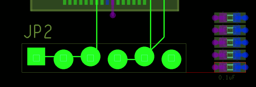
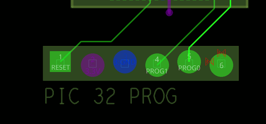
Step 31: Select the connector to attach it to your cursor. Move it such that it is in approximately the same X position but just above the start of the 0.1uF capacitors to the right of it, as shown above. Click to place the connector.
Note: The traces are adjusted automatically but are creating additional collisions with the other pins. Correct this by re-adjusting them.
Step 32: Select the Slide mode from the toolbar.
Step 33: Click to select a trace, move the mouse to adjust it, and click again to place it. Adjust the traces such that they do not intersect with any of the other pins on the connector or IC.
Step 34: Choose the Select mode from the toolbar when finished.
Confirming the Fix in 3D
Step 35: To verify the fix, open the Visibility panel and select the 3D mode.
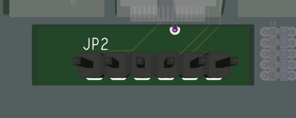
Step 36: View the connector in the 3D canvas. The connector passes through the hole in the enclosure and the error is cleared.
Wrap Up & Next Steps
Quickly find and correct 3D DRC errors with the 3DX canvas in OrCAD X Presto. Test out this feature and more with a free trial of OrCAD X Presto. For more how-tos and step-by-step walk-throughs, visit EMA Academy.
