Wilkinson Power Dividers split an input signal into two equal phase output signals. This increased isolation between the outputs prevents crosstalk, making the Wilkinson Power Divider a widespread choice for RF designs. In order to adhere to the required configuration for these circuits, transmission lines must be designed for specific impedance values, Z0 and Z0√2. With AWR, you can quickly design, simulate, and analyze transmission lines to guarantee impedance matching and achieve the expected functionality for the Wilkinson Power Divider in your RF design.
This quick how-to will provide step-by-step instructions on how to design transmission lines with specific values to meet requirements for Wilkinson Power Dividers in your RF designs with AWR Microwave Office.
How-To Video

Designing a Microstrip Transmission Line
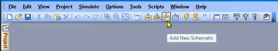
Step 1: In the AWR Design Environment and select the Add New Schematic button on the toolbar.
Note: This example will design a standard, evenly split Wilkinson Power Divider with a Z0 of 50 ohms and a Z0√2 or 70.7 ohms.
Step 2: Name the schematic Transmission Lines and click Create.
Step 3: To place a transmission line, select the Elements tab.
Step 4: Expand Microstrip and click to select Lines.
Note: Models for Microstrip lines have been expanded below the Elements list.
Step 5: Click and drag the MLIN, Microstrip Line (Closed Form) from the Models list into the schematic.
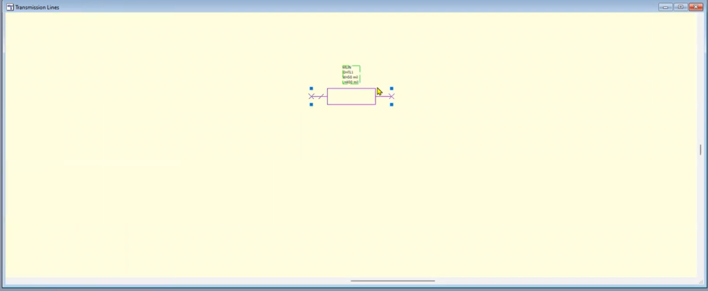
Step 6: Release the mouse. Move and orient the microstrip on the schematic canvas as desired, then click to place the Microstrip Line model.
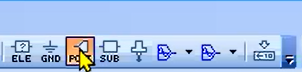
Step 7: Select the Port button from the toolbar.
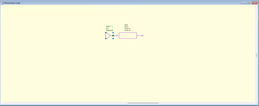
Step 8: Click to place the port at the left connection of the microstrip line model.
Step 9: Select the Port button from the toolbar.
Step 10: Press CTRL on the keyboard and right-click the mouse to vertically flip the port.
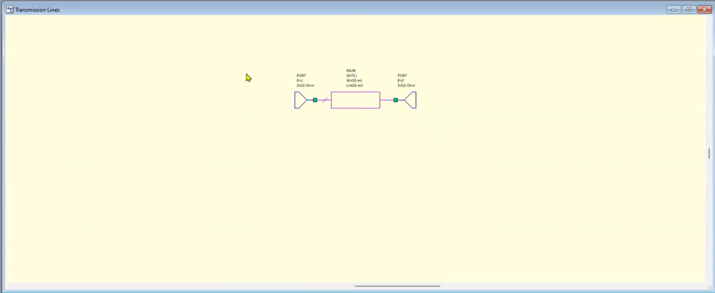
Step 11: Click to place the port at the right connection of the microstrip line model.
Note: This configuration will design a 50-ohm transmission line by adjusting the width of the microstrip model to match the 50-ohm ports.
Designing a Secondary Microstrip Transmission Line
Step 12: Press CTRL-A on the keyboard to select the current transmission line configuration.
Step 13: Press CTRL-C to copy the transmission line configuration and CTRL-V to paste.
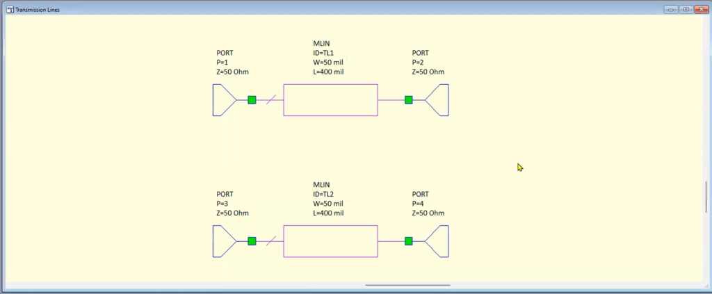
Step 14: Click the schematic to place the transmission line.
Note: To match the microstrip model to a different impedance value, the Port impedance needs to be adjusted to reflect the Z0√2 as defined in the Wilkinson Power Divider configuration.
Viewing Built-in Functions in AWR
Step 15: Select Help > Contents and Index from the menu.
Step 16: Select the Index Tab.
Step 17: In the search field, type equ to find the equations included with the AWR design software.
Step 18: Select built-in functions from the search results.
Step 19: Double-click the first Equation listed in the pop-up window.
Step 20: View the list of available mathematical equations and identify the required syntax for the square root function, sqrt(x).
Note: This index can be used to identify various built-in functions and variables to expedite RF design and analysis in AWR.
Step 21: Close the Contents and Index Window.
Configuring the Secondary Transmission Line
Step 22: Back in the schematic, click to select Port 3.
Step 23: Hold down the SHIFT key on the keyboard and click to select Port 4.
Step 24: Double-click on either of the selected Ports to open the Element Options window.
Step 25: In the Element Options window, click the cell for the Z value (50).
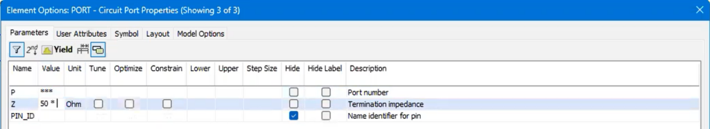
Step 26: Modify the value to be 50 * sqrt(2) and click Enter.
Step 27: Click OK.
Note: The impedance (Z) value on the schematic has been updated for both Port 3 and Port 4 which will match the microstrip line impedance to the defined port impedance of 50 * sqrt(2) Ohm.
Configuring the Substrate Definition
Note: A substrate definition is required to accurately calculate the microstrip width necessary to perfectly match impedance as the materials and thicknesses of the substrate configuration affect impedance.
Step 28: Right-click on either of the microstrip transmission lines and select Add Model Block.
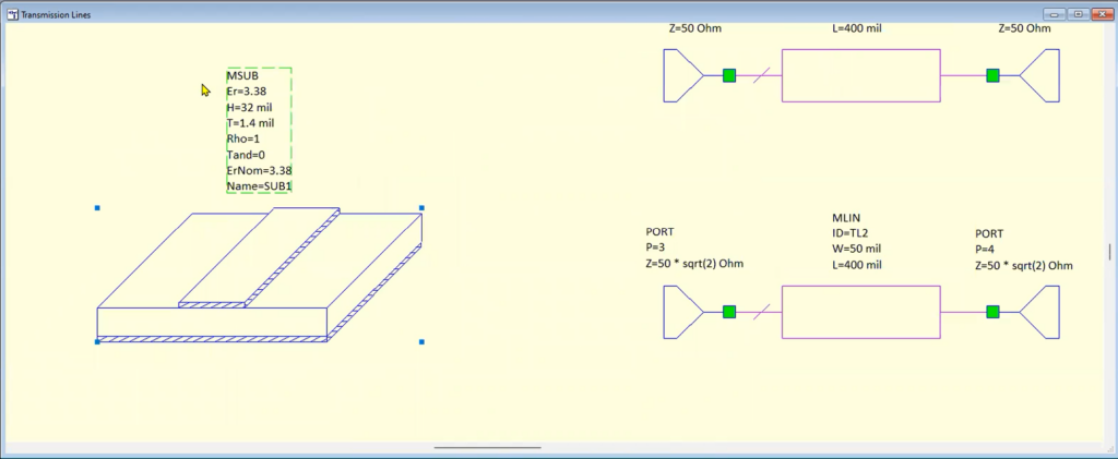
Step 29: Click to place the Model Block in the schematic.
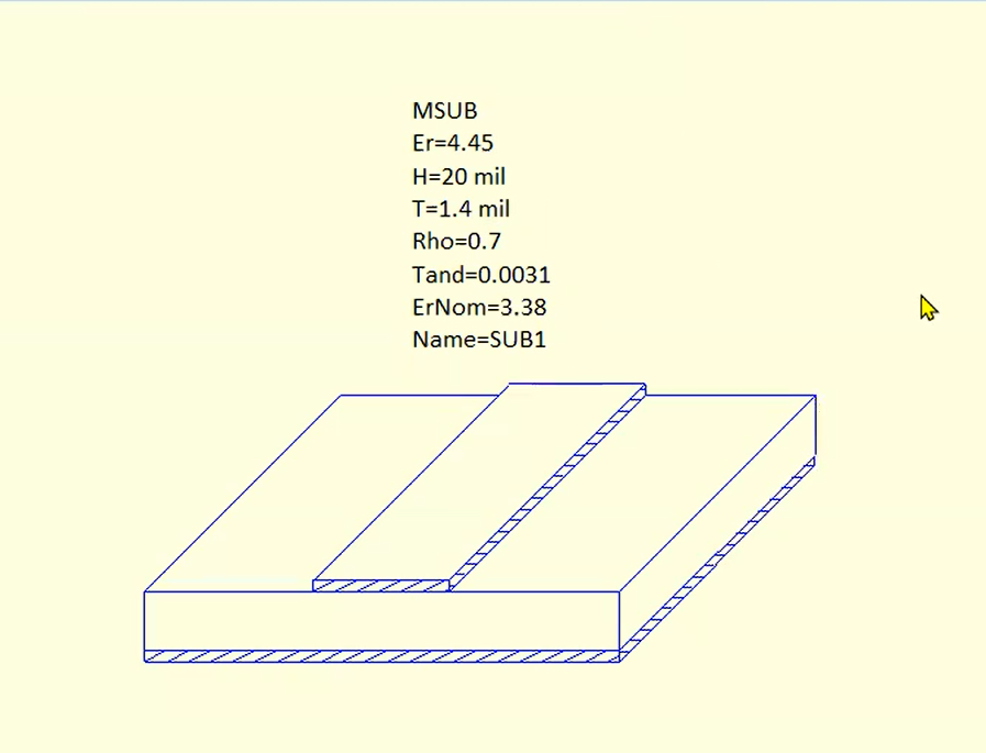
Step 30: Select the value for Er and enter a value of 4.45. Press Tab on the keyboard to be brought to the next parameter value.
Note: This will configure the dielectric coefficient to be that of FR4 material. To move up in the parameters list, use SHIFT + TAB on the keyboard.
Step 31: Enter a value of 20 for H to configure a 20mil substrate and press Tab on the keyboard.
Step 32: Enter a value of 1.4 for T to configure the thickness of the metal as 1 oz. copper. Press Tab on the keyboard.
Step 33: Enter a value of 0.7 for Rho to configure the conductivity for copper. Press Tab on the keyboard.
Note: By default, Rho is configured as the conductivity value for gold.
Step 34: Enter a value of 0.0031 for Tand to configure the dielectric tangent. Press Enter on the keyboard.
Note: This example is not performing electromagnetic analysis; therefore, the parameter ErNom does not need to be configured and can be ignored.
Defining a Frequency Range
Step 35: Select Options > Project Options from the menu.
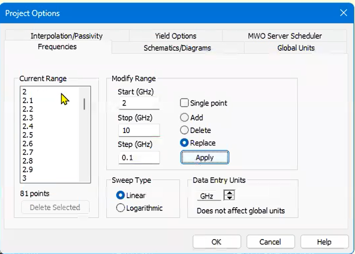
Step 36: Enter the following parameters to define the frequency for the project:
- Start: 2 GHz
- Stop: 10 GHz
- Step: 0.1 GHz
Step 37: Select Apply.
Note: The frequency range has been populated in the Current Range.
Step 38: Click OK.
Configuring Graphical Results
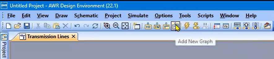
Step 39: Select the Add New Graph button from the toolbar.
Step 40: Select Smith Chart from the graph types and click Create.
Note: A Smith Chart is ideal for impedance matching because it provides an easy-to-understand, visual representation of the impedance for each transmission line.
Step 41: Right-click on the graph and select Add New Measurement.
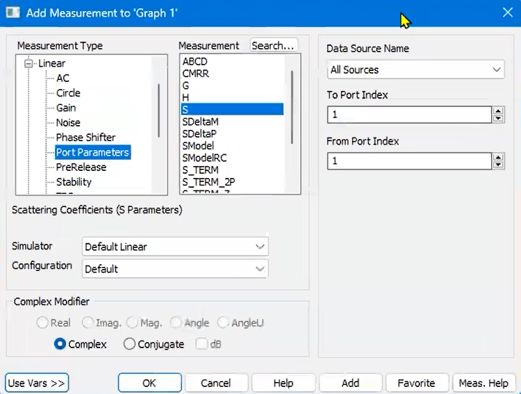
Step 42: In the Add Measurement window, select Port Parameters as the Measurement Type and S as the Measurement.
Step 43: From the Data Source Name drop down, select Transmission Lines.
Step 44: Ensure the To Port Index and From Port Index are both configured as 1 and click Add.
Note: This will configure the measurement of S11 on the Smith Chart.
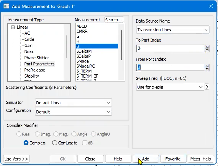
Step 45: Select the up arrow twice for the To Port Index to define a value of 3.
Step 46: Select the up arrow twice for the From Port Index to define a value of 3 and click Add.
Note: This will configure the measurement of S33 on the Smith Chart.
Step 47: Select Close.
Step 48: Select Window > Tile Vertical from the menu to adjust a split screen configuration with the schematic and Smith Chart for improved visibility.
Performing Transmission Line Analysis
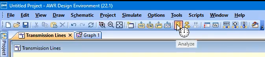
Step 49: Select the Analyze button from the toolbar.
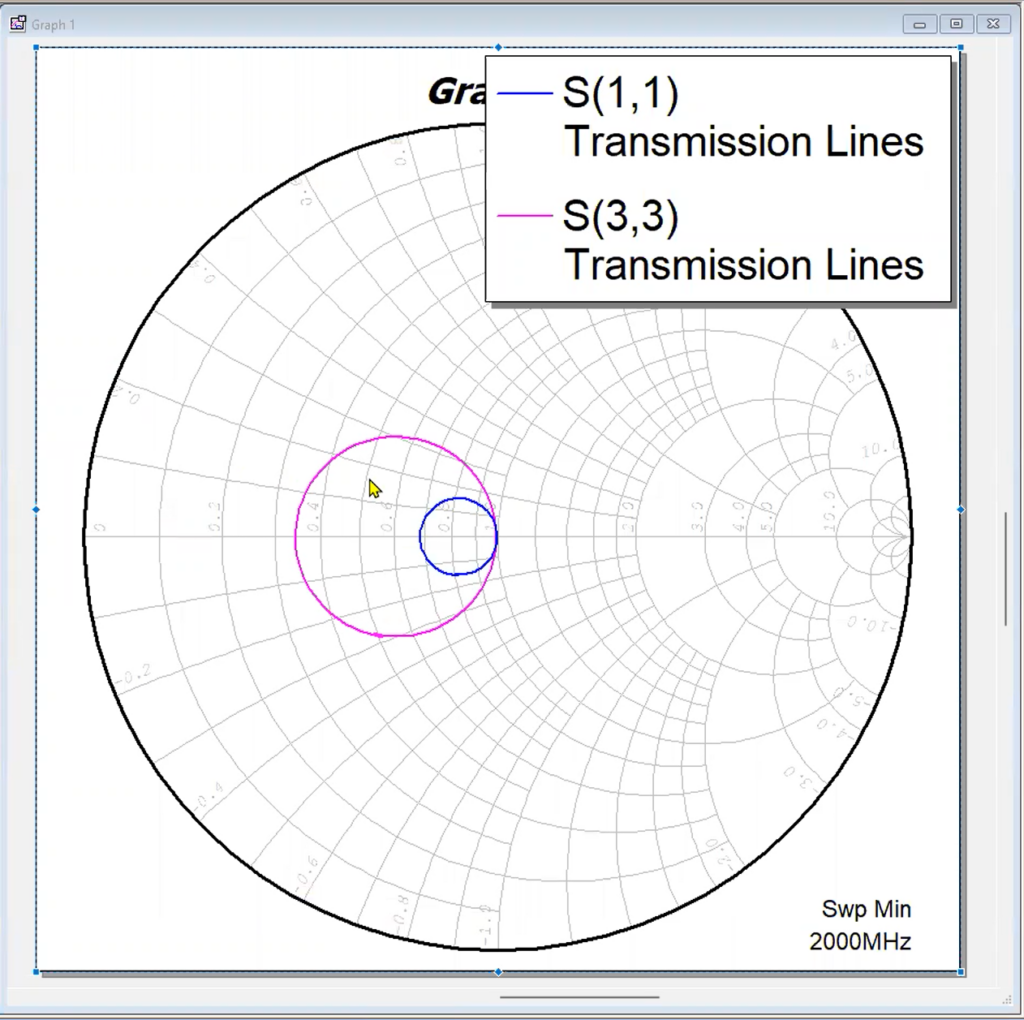
Step 50: View the results. The Smith Chart has been populated with the values for S(1,1) and S(3,3). The results for both measurements are displayed on the left of the chart, indicating impedance values for both transmission lines are lower than the target impedance.
Note: In this example, the impedance of the microstrip transmission lines needs to be increased by decreasing the width.
Modifying the Transmission Line Models
Step 51: Click to select one of the microstrip models.
Step 52: Press SHIFT on the keyboard and click to select the other microstrip model.
Step 53: Double-click one of the models to edit the element options.
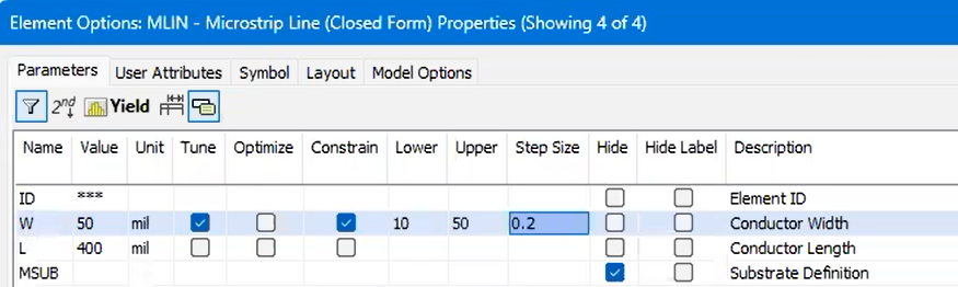
Step 54: In the width (W) row, check the box for Tune.
Note: This will allow the width to be tunable.
Step 55: In the width (W) row, check the box for Constraint.
Step 56: Select the Lower cell and set a constraint value of 10. Use the right arrow key on the keyboard to move to the next cell.
Step 57: Enter a value of 50 for the Upper constraint and press the right arrow key on the keyboard.
Step 58: Enter a value of 0.2 for the Step Size and press the right arrow key on the keyboard.
Note: This will ensure the microstrip width is set between 10mils and 50mils. The value of the width will be determined with a 0.2mil granularity.
Step 59: Select OK.
Note: In the schematic, the width parameter of both MLIN transmission models have turned blue indicating this value is now tunable.
Tuning Transmission Line Models
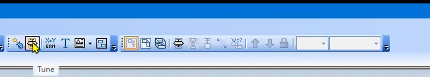
Step 60: Select the Tune button on the toolbar.
Note: This displays both microstrip transmission line models with the tuning constraints visible.
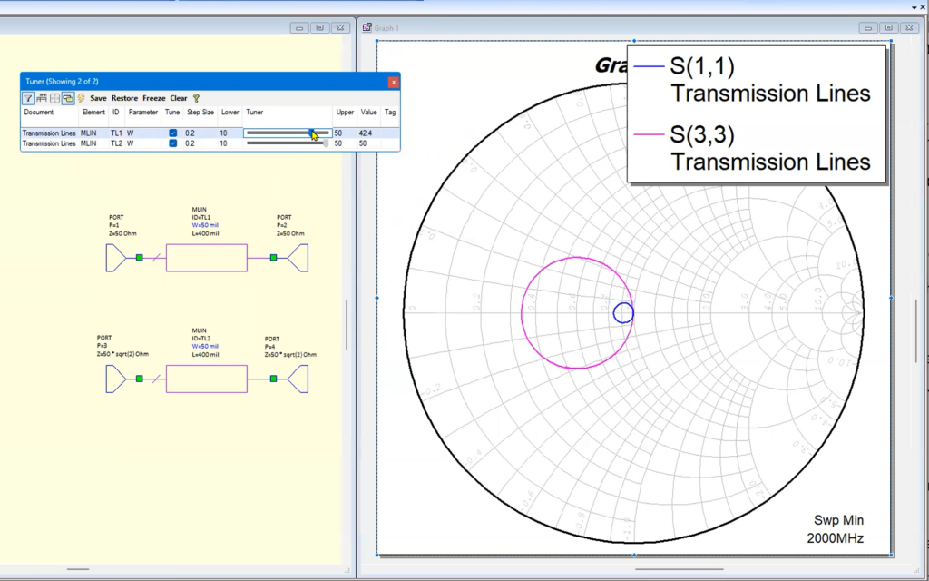
Step 61: Select the slide bar under Tuner for TL1 and drag the marker to tune the transmission line.
Note: With the adjustment of the tuning meter, the blue curve moves closer to the center of the Smith Chart.
Step 62: Move the tuning meter until the measurement on the Smith Chart becomes zero, approximately 36.8 mils.
Step 63: Select the slide bar under Tuner for TL2 and drag the marker to tune the transmission line.
Note: With the adjustment of the tuning meter, the pink curve moves closer to the center of the Smith Chart.
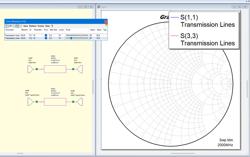
Step 64: Move the tuning meter until the measurement on the Smith Chart becomes zero, approximately 18.6 mils.
Step 65: Click the X to close the tuning window.
Step 66: In the Smith Chart, hold the CTRL key and roll the wheel on your mouse to zoom into the center for a more detailed view of the TL1 and TL2 measurements.
Note: View > Zoom from the menu and the zoom buttons on the toolbar can also be used to zoom in or out of the schematic canvas and Smith Chart results.
Wrap Up & Next Steps
Easily design transmission lines to ensure impedance matching and proper functionality of Wilkinson Power Dividers using the efficient RF schematic design and analysis capabilities of the AWR Design Environment.

