A well-designed low pass filter is key in any RF design. Filters need to suppress not only unwanted noise from higher frequencies, but crosstalk as well. If not designed carefully, the low pass filter can lose its effectiveness and negate any shielding, which could have a detrimental effect on RF circuit performance. With AWR, you can quickly design a low-pass filter to guarantee proper bandpass and band stop behavior in your RF design.
This quick how-to will provide step-by-step instructions on how to design a low-pass filter in your RF designs using a wizard-based approach in AWR Microwave Office.
How-To Video
 Open in New Window
Design a Low-Pass Filter
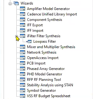
Step 1: Select the Project tab in the AWR Design Environment.
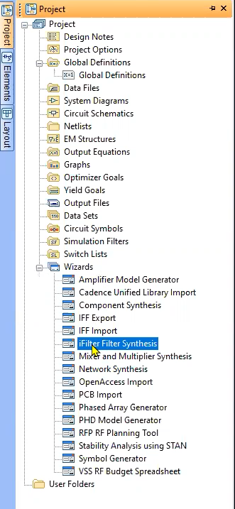
Step 2: Expand Wizards and select iFilter Filter Synthesis.
Note: iFilter Filter Synthesis provides a wizard-based approach to designing filters with an easily customizable design environment and real-time feedback.
Step 3: Select Design for the synthesis mode.
Step 4: Select Lowpass for the Passband and Microstrip for the Realization.
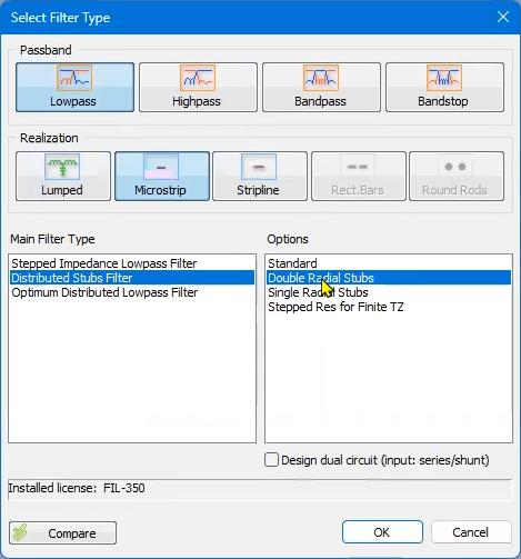
Step 5: Select Distributed Stubs Filter as the Main Filter Type and Double Radial Stubs for the options. Click OK.
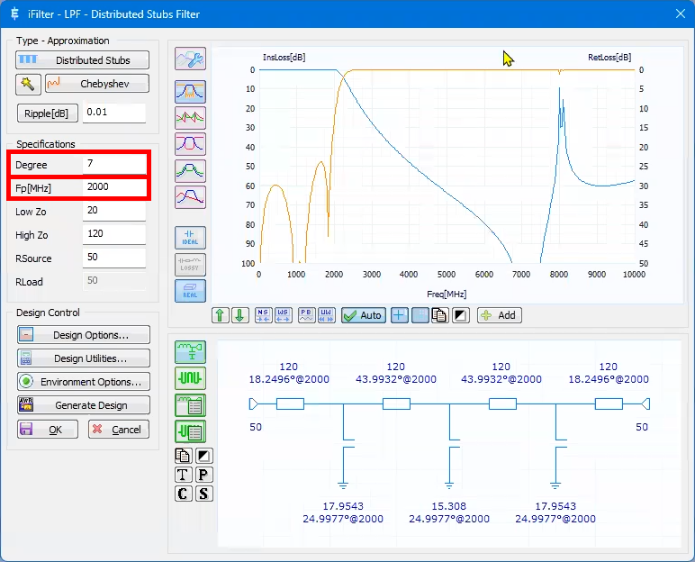
Note: The iFilter wizard window opens, showing the basic filter design and expected performance. This filter has seven poles and a lowpass frequency of 2GHz.
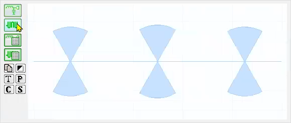
Step 6: Select the Layout button to view the layout.
Defining the Substrate
Step 7: Select Design Options to configure the substrate definition.
Note: Substrate must be defined before the circuit can be generated.
Step 8: Select the Technology tab.
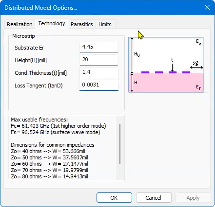
Step 9: Set the following parameter values:
- Substrate Er: 4.45
- Height: 20mil
- Conductor Thickness: 1.4
- Loss Tangent: 0.0031
Note: These values correspond to an FR-4 substrate.
Step 10: Click OK.
Setting Optimization Goals
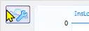
Step 11: Click the Chart Settings button at the top of the window.
Step 12: Select Opt Goals in the Chart Settings window.
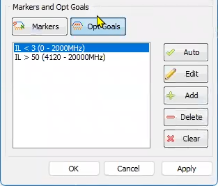
Step 13: Confirm that the passband, indicated by IL < 3 (0-2000MHz); and stop band, indicated by IL > 50 (4120-20000MHz) are present in the Opt Goals list.
Step 14: Click Apply and OK. The goals will appear in the performance plot and be sent to the schematic when it is generated.
Creating the Schematic
Step 15: Select Generate Design. The Generate Schematic window opens.
Step 16: Name the schematic Lowpass Filter.
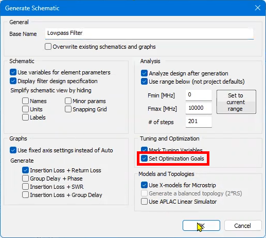
Step 17: Check the option to Set Optimization Goals. Click OK.
Step 18: Click OK in the iFilter window to close it. This will save the Lowpass Filter schematic in the project tree under iFilter Filter Synthesis.
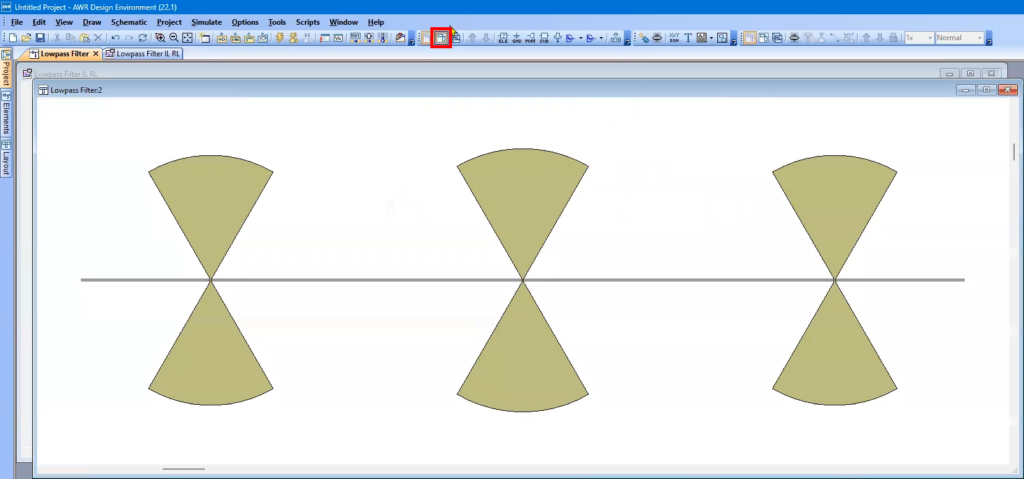
Step 19: View the generated schematic and filter performance based on the schematic analysis.
Step 20: Select the Layout button from the toolbar to view the layout.
Changing the Substrate Resistivity
Step 21: In the schematic window, zoom into the substrate. Double-click the substrate symbol to open the Element Options window.
The Description for Rho shows that the resistivity has been normalized to gold; therefore, the value of 1 for Rho indicates that the metal is defined as gold.
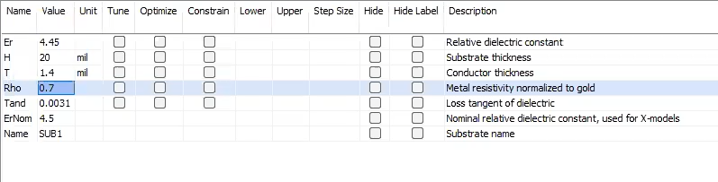
Step 22: Double-click the value for Rho and change the value to 0.7. Click OK. This will configure the resistivity for copper (0.7).
Note: The plots of the filter performance are now dimmed to indicate the analysis needs to be performed again.

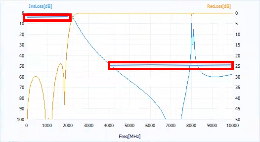
Step 23: Select the Analyze button on the toolbar to rerun the analysis. The filter performance graph is updated and the filter output passes above the desired insertion loss around 8GHz.
Step 24: Select Windows > Tile Vertical to view all open result windows together.
Optimizing the Design
Step 25: Select Simulate > Optimize from the menu.
Step 26: The Optimizer window opens. Click Start to run the optimization.
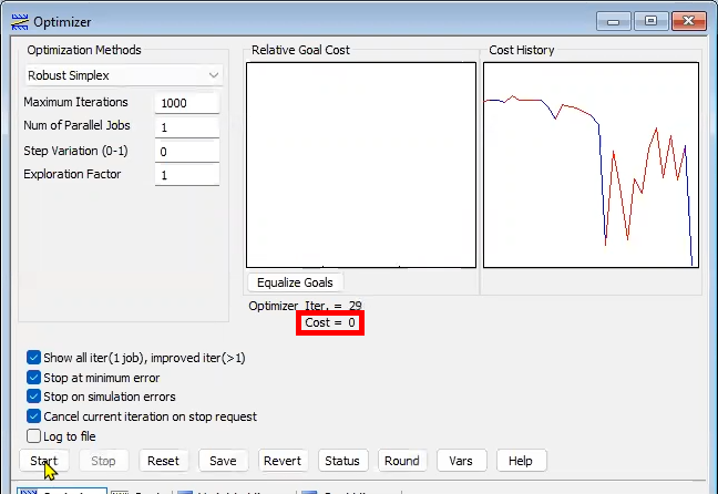
Step 27: View the Optimization. The optimization finishes with a cost of 0, indicating there are no longer errors in the filter design. The filter output now remains under the desired insertion loss for the entire stop band and both goals are achieved.
Step 28: Close the Optimizer and zoom into the layout view. Red Xs are visible, indicating that the parameters have changed.
Step 29: Press CTRL-A on the keyboard to select everything.

Step 30: Select the Snap Together button from the toolbar. The Xs are removed as the windows are synced.
Measuring the Through Line
Note: The schematic views each piece of the layout individually; therefore, electromagnetic analysis should be performed to analyze the complete functionality including possible coupling between parallel or open stubs. To run electromagnetic analysis, the thickness of the narrowest line or the through line, must be measured.
Step 31: Zoom into the through line, between the first two stubs, in the layout view.

Step 32: Select the Measure button from the toolbar or press CTRL-D on the keyboard to activate measurement mode.
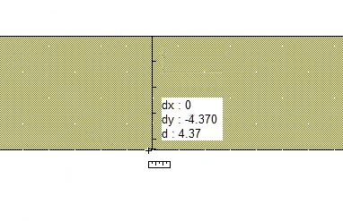
Step 33: Click and drag in the layout view from the top of the line to the bottom. In this case, the line is 4.37 mils wide.
Note: In electromagnetic analysis, the mesh should be set to 10% of the narrowest line. In this example, 4.37 will be rounded to 5 mils and the mesh will be configured as 0.5 mils.
Step 34: Zoom back out to the full layout view.
Preparing Electromagnetic Analysis
Step 35: Click to select the schematic as the in-focus window.
Step 36: Select Scripts > EM > Create Stackup from the menu.
Step 37: In the Axiem Setup window, enter 0.5 mil for the Grid size.
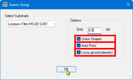
Step 38: Ensure Union Shapes, Auto Ports, and Lossy Ground Planes checked and click OK.
Note: Two elements are added to the schematic:
- Substrate stackup
- Extract block
These elements include information on the EM structure and information that will be set up during the simulation regarding substrate and materials. For more information, double-click the block. The substrate block provides more information including:
- Material Definitions
- Dielectric Layers
- EM Layer Mapping
- Line Type
- Parameters
Step 39: Click and drag to select all original elements in the schematic to enable them for EM simulation.
Note: Hold Shift while dragging to select objects even if they are not completely enclosed in the selection box.
Step 40: Double-click any of the selected items to open the Properties window.
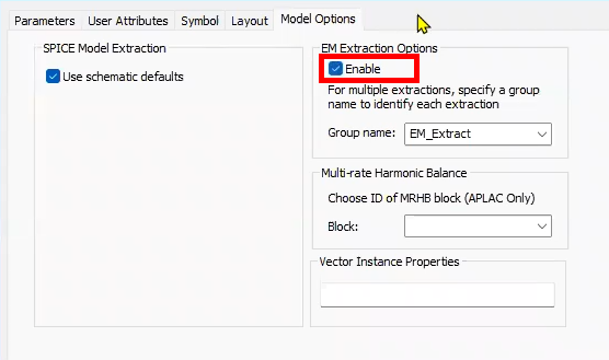
Step 41: Select the Model Options tab and check Enable under EM Extraction Options.
Step 42: Click OK.
Note: All schematic elements will be enabled for EM extraction. To check what is enabled, select the extract block. The enabled schematic elements and layout stubs are highlighted in red.
Running Electromagnetic Analysis
Step 43: Right-click the extract block and select Add Extraction.
A window opens showing a similar layout plot. This is the EM setup, with ports at either end. The “A” signifies an automatic port, the mesh will be automatically removed after the analysis.

Step 44: With the extract block window still open, select Show 2D Mesh from the toolbar.
Step 45: Zoom into the narrow connecting line. The mesh is 10% of the line’s thickness, as defined earlier.
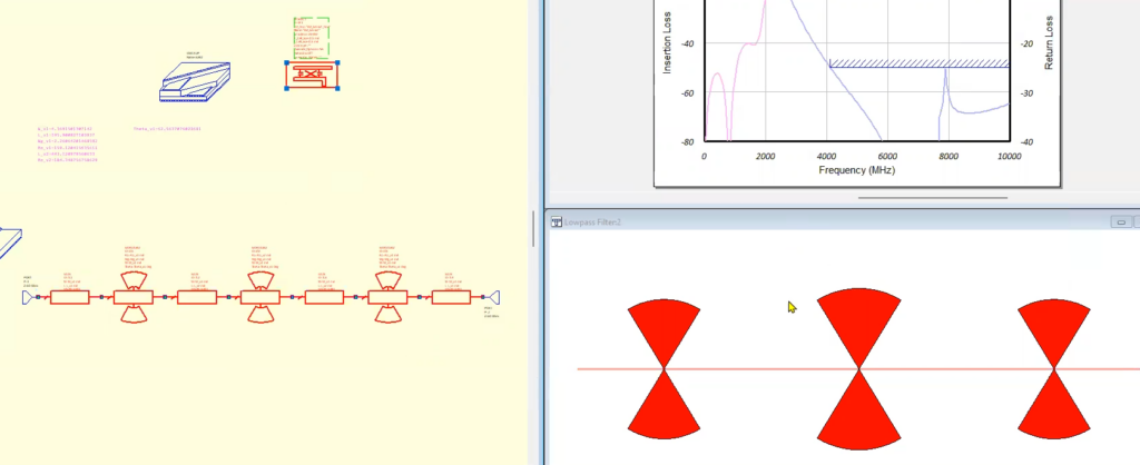
Step 46: Select Window > Tile Vertical from the menu.
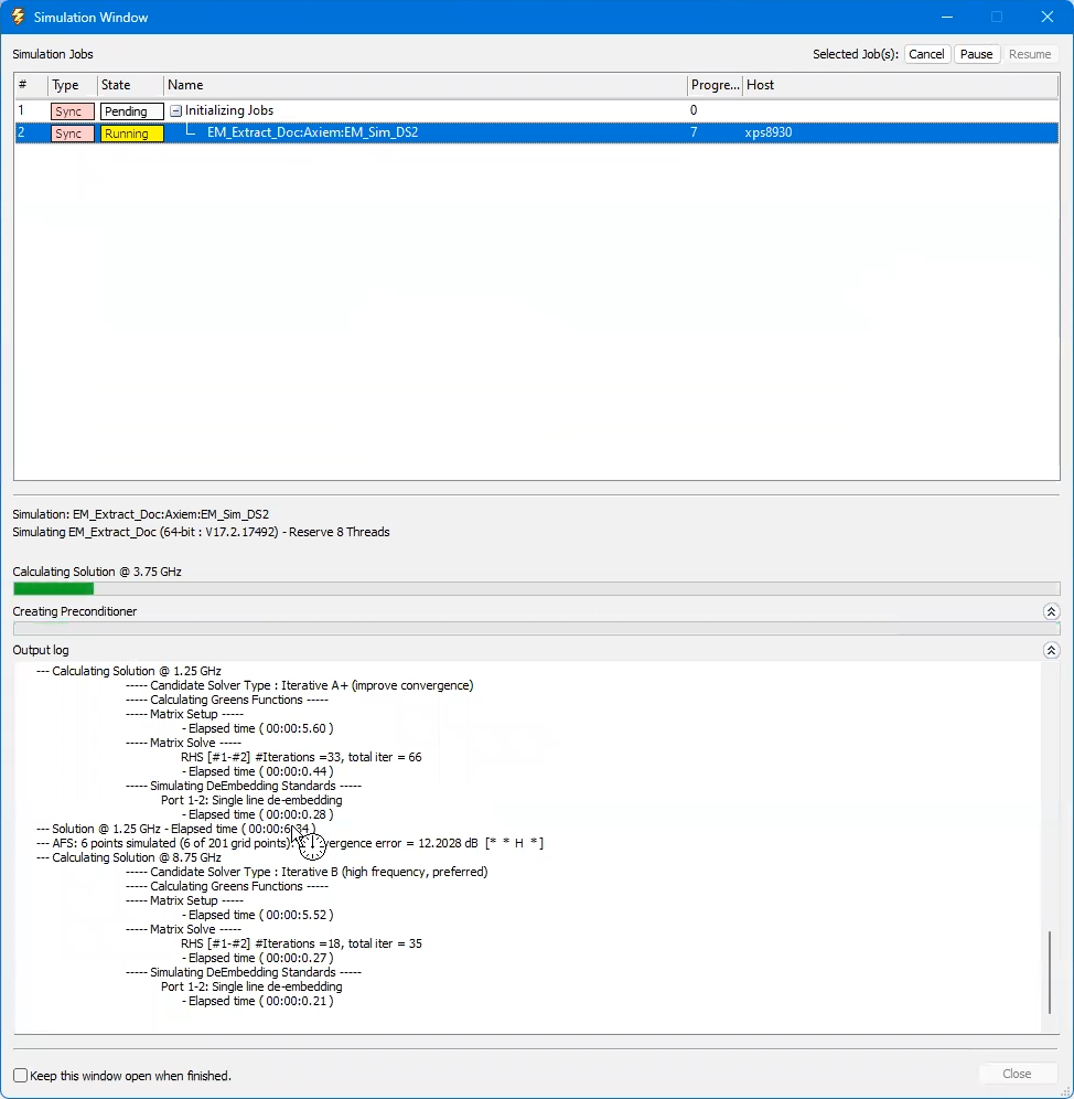
Step 47: Select Analyze to run the EM analysis. An output log is shown during the simulation. The simulation will be run until the convergence error is less than -30dB.
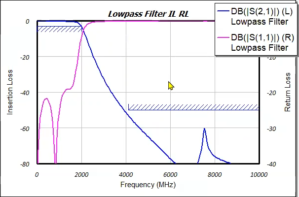
Step 48: When the simulation finishes, view the results. The performance plot has been updated to reflect any crosstalk between stubs, which was not plotted with the standard schematic simulation. Both the bandpass and band stop goals are still met.
Comparing Analysis Results
Step 49: Select the Maximize button to make the performance plot full screen.
Note: Click and drag to adjust the legend as needed.
Step 50: Select the Freeze Traces button from the toolbar.
Step 51: Select the Lowpass Filter:1 tab to view the schematic. Right-click the extract block and select Toggle Enable. This will disable EM analysis.
Step 52: Select Analyze.
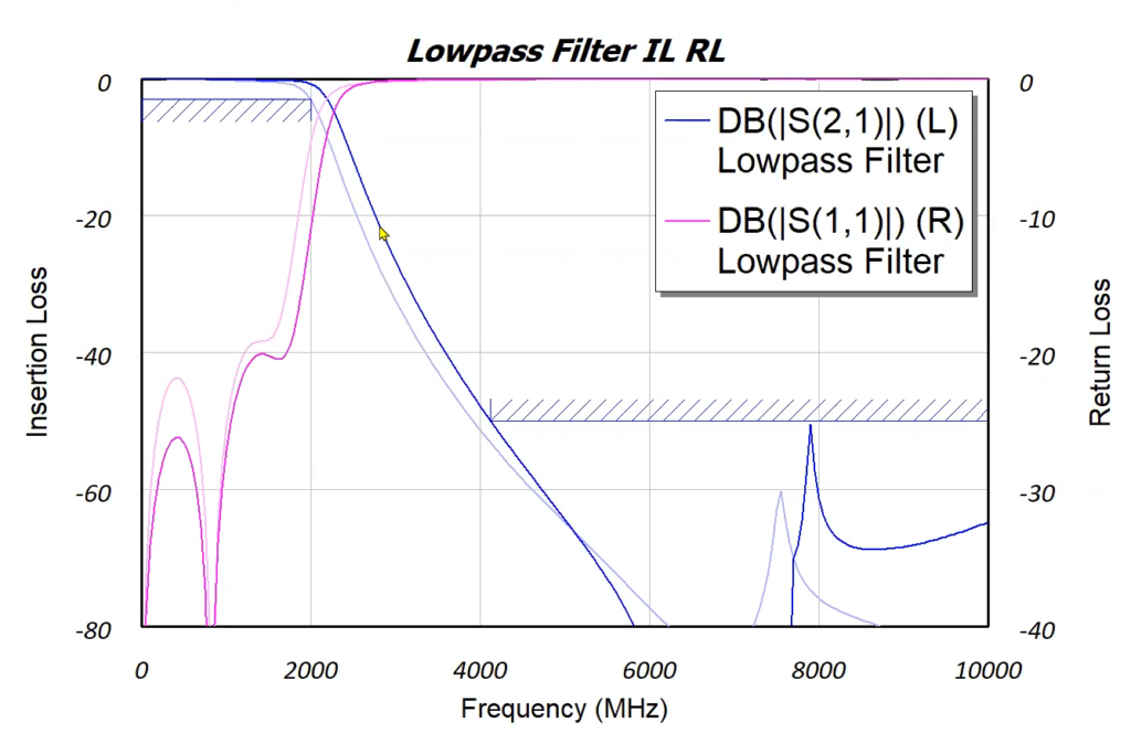
Step 53: View the plot. The schematic analysis results are shown with the EM results slightly faded out for efficient comparison.
Wrap Up & Next Steps
Easily design a low-pass filter using the efficient RF schematic design and analysis capabilities of the iFilter Filter Synthesis wizard in the AWR Design Environment. Test out this feature and more with a free trial of AWR and get more step-by-step how-tos at EMA Academy.

