As designs increase in speed and become more compact, the ability to efficiently route differential pairs to minimize noise is more important than ever. For optimal signal integrity, differential pairs must first be defined to utilize rules to ensure accurate routing. With OrCAD PCB Designer, quickly define differential pairs during the PCB layout manually and automatically to accelerate routing and improve signal integrity throughout your design.
This quick how-to will provide step-by-step instructions on how to define differential pairs in OrCAD PCB Designer.
To follow along, download the provided files above the table of contents.
How-To Video

Defining Differential Pairs Manually
Step 1: Open the provided design in OrCAD PCB Designer.
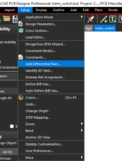
Step 2: Select Setup > Add Differential Pairs from the menu.
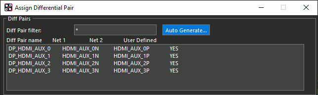
Step 3: Select HDMI_AUX_0N and HDMI_AUX_0P from the nets list.
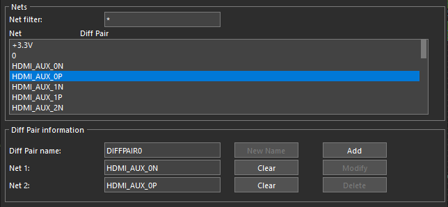
Note: These nets are added to the Diff Pair Information panel automatically.
Step 4: Enter DP_HDMI_AUX_0 into the Diff Pair Name field.
Step 5: Click Add. The differential pair has been added to the Diff Pairs list at the top of the window.
Step 6: Select nets HDMI_AUX_1N and HDMI_AUX_1P.
Step 7: Enter DP_HDMI_AUX_1 into the Diff Pair Name field and click Add.
Step 8: Select nets HDMI_AUX_2N and HDMI_AUX_2P.
Step 9: Enter DP_HDMI_AUX_2 into the Diff Pair Name field and click Add.
Step 10: Select nets HDMI_AUX_3N and HDMI_AUX_3P.
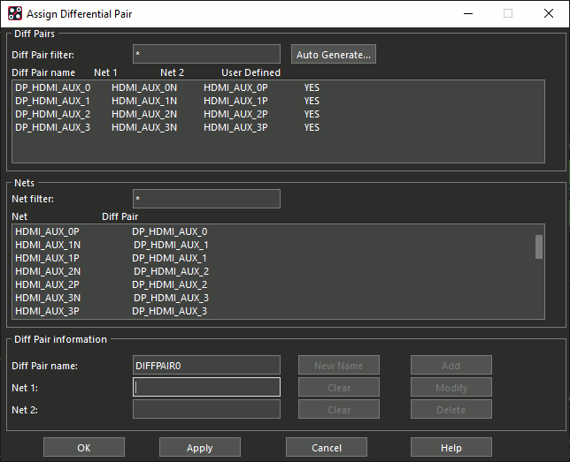
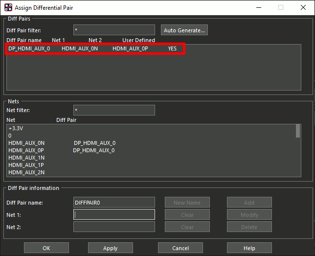
Step 11: Enter DP_HDMI_AUX_3 into the Diff Pair Name field and click Add. The HDMI_AUX nets have been defined.
Defining Differential Pairs Automatically
Step 12: Select Auto Generate in the Diff Pairs list.
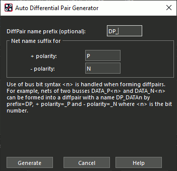
Step 13: The Auto Differential Pair Generator opens. Enter DP_ for the prefix, P for the + Polarity, and N for the – Polarity.
Note: By entering a prefix for the differential pair, the differential pair nets can be easily identified throughout the PCB design.
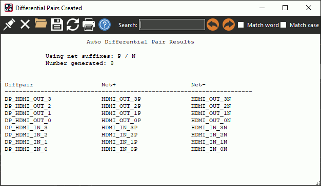
Step 14: Select Generate. A log window opens showing the differential pairs created. Review and close the window.
Step 15: Click OK in the Assign Differential Pair window to save the settings and close the window.
Verifying Differential Pair Assignments
Step 16: Select Setup > Constraints from the menu or the Constraint Manager button from the toolbar.
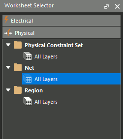
Step 17: Select the Physical domain from the Worksheet Selector and select the Net > All Layers worksheet.
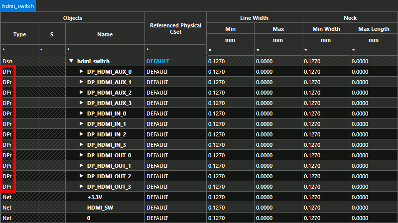
Step 18: View the constraint table. All HDMI net pairs are grouped into their appropriate differential pair groups, indicated by type DPr.
Step 19: Close the constraint manager window.
Routing Differential Pairs
Step 20: Select Route > Connect from the menu.
Step 21: Select net HDMI_IN_0P or HDMI_IN_0N from connector J1.
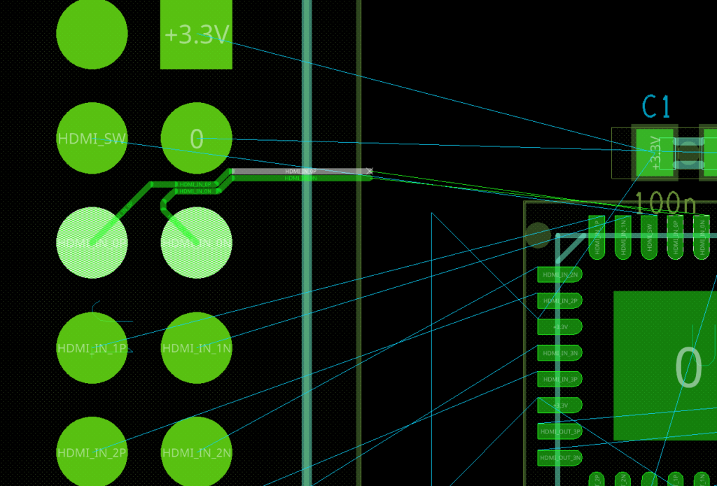
Step 22: Click to start routing the connection. By selecting one net of the differential pair both traces are activated to route them together.
Note: Be sure to set the required constraints for the differential pairs. When constraints are configured the line width, gap, and critical parameters of the differential pair will be automatically adhered to when routing.
Wrap Up and Next Steps
Easily define differential pairs during the PCB layout to ensure accurate routing with manual and automatic differential pair assignment in OrCAD PCB Designer. Test out this feature and more with a free trial of OrCAD.

