With RF designs, accurate trace impedance is critical to signal integrity and circuit performance. At high frequencies, the soldermask that covers the etches can affect the impedance and functionality of the RF circuitry. Quickly create soldermask openings for RF traces with the Cross Copy feature in Allegro Productivity Toolbox. Cross Copy provides additional flexibility and allows you to quickly copy and change features between classes on the PCB. With the productivity toolbox, you can:
- Copy a trace segment to a non-etch subclass
- Copy shapes on manufacturing and drawing subclasses
- Copy text between layers
- Specify layers for the objects to be copied
- Export drill information into artwork (donuts)
This how-to will provide step-by-step instructions on how to use the Cross Copy feature in Allegro Productivity Toolbox to quickly create soldermask openings for RF signals. To follow along, use the provided design above the table of contents.
How-To Video

Activating Cross Copy
Step 1: Open the provided design in OrCAD PCB Designer Professional with the Allegro Productivity Toolbox option selected.
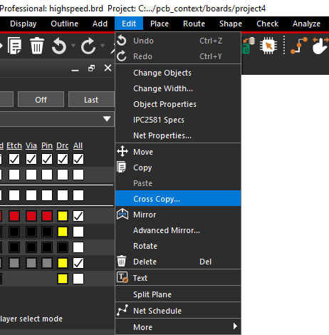
Step 2: Select Edit > Cross Copy from the menu.
Configuring Cross Copy Parameters
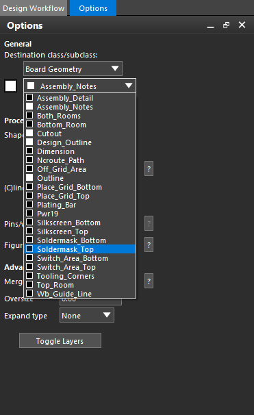
Step 3: In the Options panel, select Board Geometry as the active class and Soldermask_Top as the active subclass.
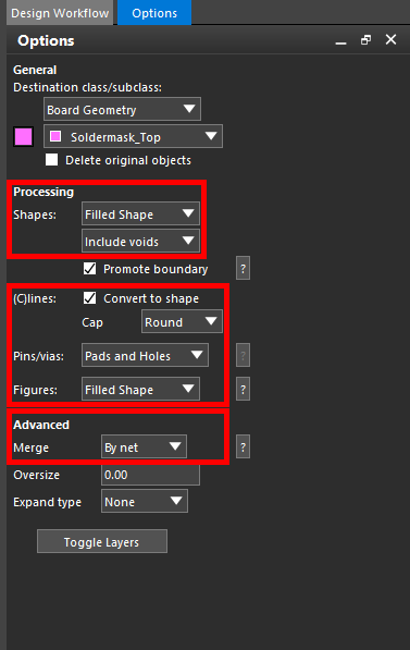
Step 4: Under Processing, set the Type to Filled Shape and the Voids option to Include voids.
Note: The type can be set as the following options:
- Filled Shape: With this option, a filled shape will be created on the destination layer. When voids are included, a one-to-one copy will be created on the destination layer. When voids are excluded only the shape boundary will be copied as filled shape to the destination layer.
- Unfilled Shape: With this option, only the shape boundary will be copied as unfilled shape. Any voids will be ignored.
- Decompose: With this option, the shape will be decomposed to the destination layer. You have the choice to include or exclude voids during the operation.
Step 5: Check Convert to Shape.
Note: This will convert cline and line objects to shapes.
Step 6: Set the Cap to Round.
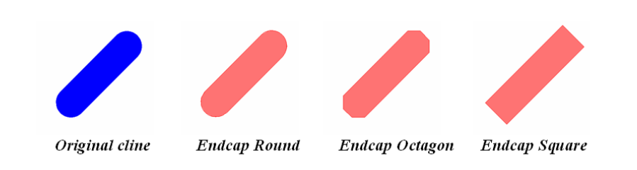
Note: For Cap, select from Square, Round, or Octagon Endcap styles.
Step 7: Set the Pins/Vias mode to Pads and Holes and the Figures mode to Filled Shape.
Note: When processing pins and vias select from the following:
- Pads Only: In this mode, the pad dimensions are extracted and an equivalent shape will be drawn on the destination layer. The drill hole will be ignored.
- Holes only: In this mode, a positive shape of the drill hole only is created on the destination layer. Pad shapes are completely ignored.
- Pads and Holes: In this mode, the pad dimensions are extracted and an equivalent shape will be drawn on the destination layer. Drill holes will be added as voids to the shape.
Step 8: Under Advanced, select By Net from the Merge drop-down menu.
Note: With this option, only data will be merged where objects belong to the same net (pin, vias, clines and shapes, depending on find filter settings).
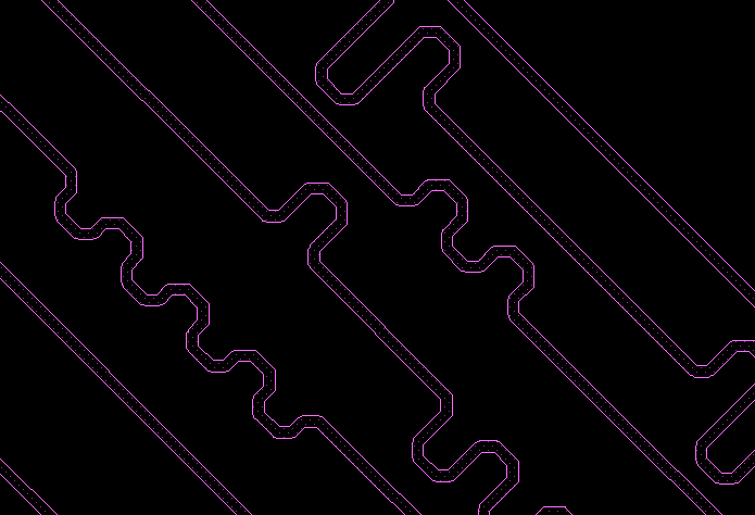
Creating Soldermask Openings
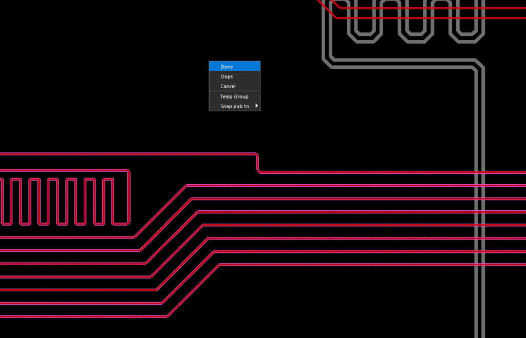
Step 9: Select the traces to be opened. Right-click and select Done when finished.
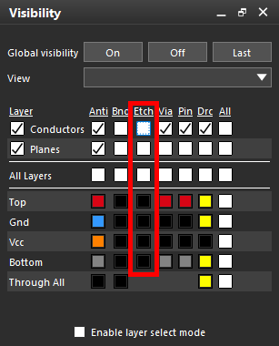
Step 10: In the Visibility panel, un-check all Etch layers to show the soldermask.
Wrap Up & Next Steps
Efficiently copy objects and features on the PCB between different classes and subclasses to quickly complete the PCB layout. To learn more about how the features of Allegro Productivity Toolbox can expedite your PCB designs, view our latest webinar.

