The key to success with any circuit is a solid connection to power and ground. Robust connections are typically made through power and ground planes on otherwise unused layers of the board. Additionally, power-hungry sections of the board may require copper shapes on main board layers as well. OrCAD PCB Designer provides multiple methods to create planes and copper shapes and planes efficiently.
This quick how-to will provide step-by-step instructions on how to create planes and copper pours in OrCAD PCB Designer.
To follow along, download the provided files above the table of contents.
How-To Video
 Open in New Window
Creating Copper Shapes
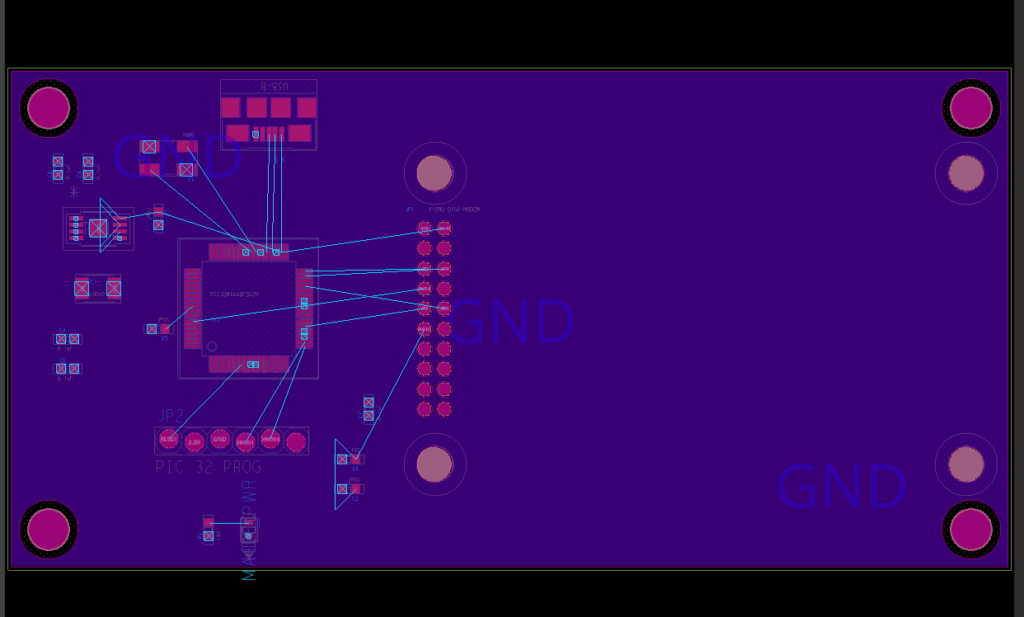
Step 1: Open the provided design in OrCAD PCB Designer.
Step 2: Select Shape > Rectangular from the menu.
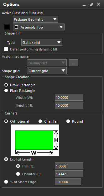
Note: The Options panel shows rectangle placement options. If this panel is not visible, select Display > Windows > Options from the menu.
Step 3: Under Active Class and Subclass, select Etch from the Active Class drop-down menu.
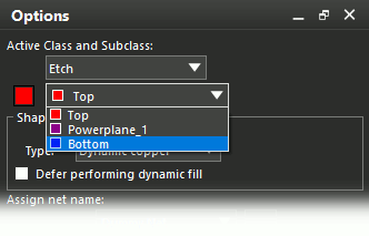
Step 4: Select Bottom from the Active Subclass menu.
Step 5: Under Assign Net Name, select the ellipsis to open the net selection window.
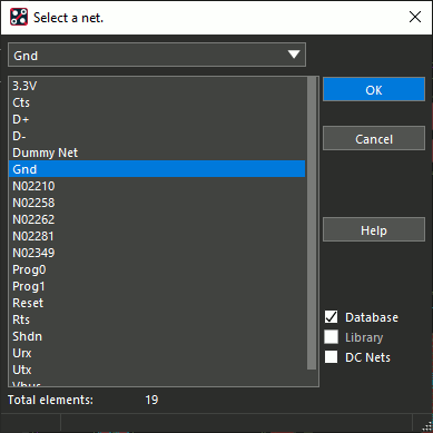
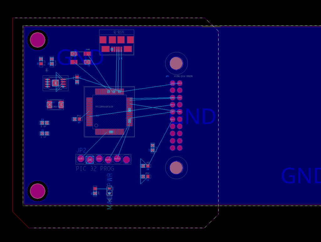
Step 6: Select Gnd from the list and click OK.
Note: The net can also be selected from the drop-down menu under Assign Net Name, which lists, the power and ground nets.
Step 7: Click in the upper-left corner of the board to start drawing the shape and click again to finish in the bottom-right corner.
Note: Any edges of the shape outside the board outline will be trimmed automatically.
Merging Copper Shapes
Step 8: Select Shape > Polygon from the menu to activate polygon options.
Step 9: Select Powerplane_1 from the Active Subclass dropdown.
Note: Etch is automatically selected as the active class from the last shape mode.
Step 10: Select the ellipsis under Assign Net Name.
Step 11: Choose 3.3V from the net list and click OK.
Step 12: Click to start drawing the shape in the upper-left corner of the board.
Note: Moving your mouse up or down will show a diagonal edge. Clicking will place the edge as shown.
Step 13: Click to add four corners around the left half of the board.
Step 14: Right-click and select Complete to close the polygon.
Step 15: Right-click and select Next to start drawing the other half.
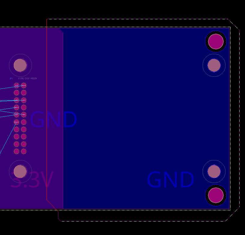
Step 16: Click to draw a polygon over the other half of the board, ensuring overlap with the first half. Right-click and select Complete when finished.
Step 17: Right-click and select Done to end the drawing mode.
Step 18: To merge the shapes into one, select Shape > Merge Shapes from the menu.
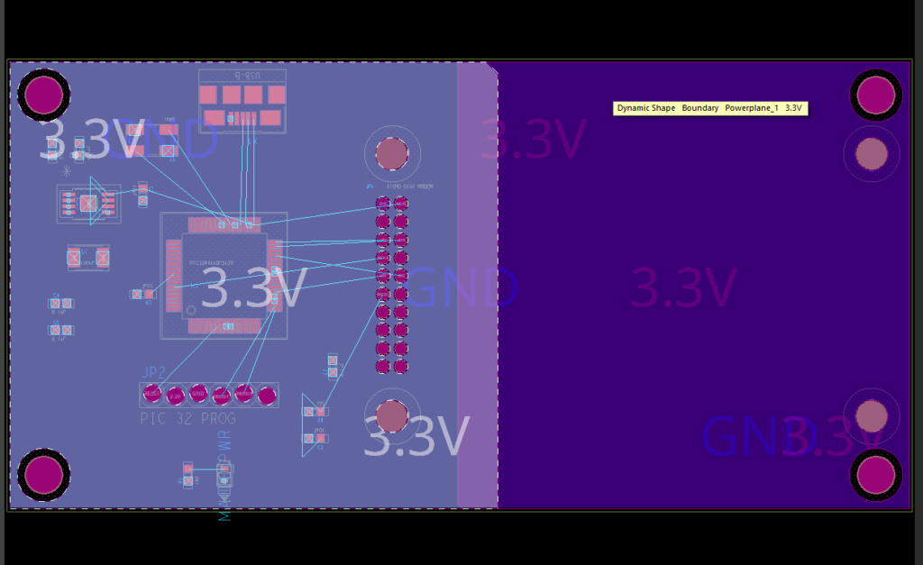
Step 19: Select the left shape, then the right shape. The shapes are merged into a single plane.
Step 20: Right-click and select Done.
Create Planes in OrCAD with Z-Copy
Note: To demonstrate Z-copy, we will delete the power plane and recreate it.
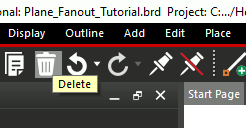
Step 21: Select Delete from the toolbar.
Step 22: Select the power plane, then right-click and select Done to delete it.
Step 23: Select Shape > Z-Copy from the menu.
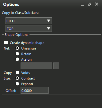
Note: The Z-Copy feature can be used to make a copy of a shape on a different layer or with an offset. The Options panel populates with Z-Copy options. Looking for the equivalent of Z-Copy in OrCAD X Presto? Learn how to achieve this functionality with the Paste Special command here.
Step 24: Select Powerplane_1 from the subclass dropdown under Copy to Class/Subclass.
Step 25: Check Create Dynamic Shape.
Note: If this option is not checked, a static shape with no healing properties is created.
Step 26: Select the ground shape, then right-click and select Done. The shape is copied to the power plane layer.
Note: While the new shape has been created in the correct layer, it is still connected to the ground net.
Step 27: Select the shape. Right-click and select Assign Net.
Step 28: In the Options panel, under Assign Net Name, select 3.3V from the dropdown. Right-click in the canvas and select Done.
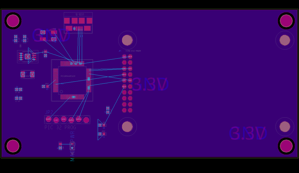
Step 29: View the canvas. The power and ground planes have been drawn and are ready to connect to the components.
Wrap Up & Next Steps
Quickly create planes and copper shapes to ensure proper power delivery and grounding in OrCAD PCB Designer. Test this feature and more with a free trial of OrCAD. Get more how-tos for OrCAD at EMA Academy.

