To create fanouts, vias are connected to pads of a component. Fanouts have many uses, making them a key element in PCB designs, including:
- Connecting to power and ground planes
In multi-layer stackups through-hole components easily connect to power and ground planes; however, surface mount components require fanouts to establish the required connections.
- Enhancing routing accessibility
Fanouts increase the space available for routing BGA and High-Density Interconnect (HDI) components. By using vias and fanouts, signals can be routed through multiple layers, allowing designers to optimize the routing of complex designs.
- Improving manufacturability and testability
For high-pin count components, incorporating fanouts ensures that PCBs can be manufactured reliably and provides accessible points for connecting test equipment during manufacturing and testing.
OrCAD PCB Designer makes it easy to create fanouts for surface mount components with fully configurable settings and automated via placement.
This quick how-to will provide step-by-step instructions on how to create fanouts in OrCAD PCB Designer.
To follow along, download the provided files above the table of contents.
How-To Video
 Open in New Window
Create Fanouts for Components in OrCAD PCB
Step 1: Open the provided design in OrCAD PCB Designer.
Step 2: To help enhance the visibility of fanouts, select the Color button from the toolbar.
Step 3: In the Layers tab, uncheck All and check Top.
Note: This will only display objects on top of the board. The power and ground planes, which span the entire board, will not be visible.
Step 4: To change the color of the individual power and ground nets, select the Nets tab.
Step 5: Select Magenta from the Available Colors table and select the 3.3V cell under Net.
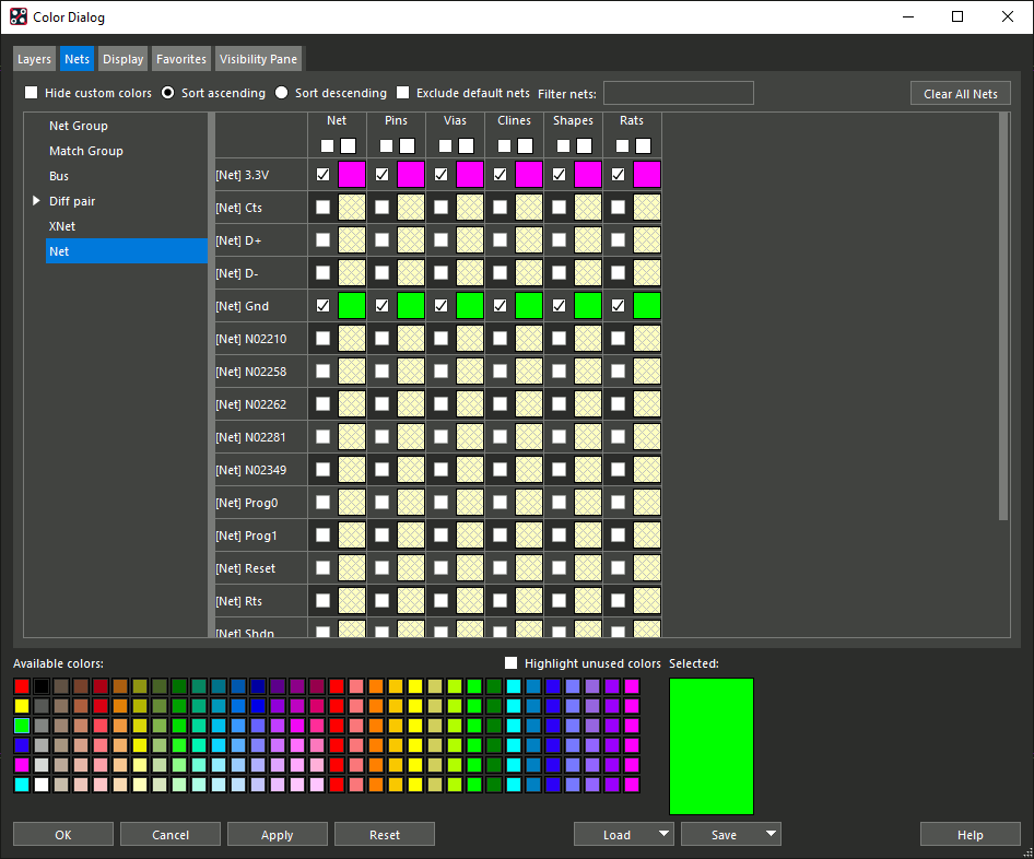
Step 6: Select Green from the Available Colors table and select the Gnd cell under Net.
Note: Assigning colors to the power and ground nets will ensure that power and ground pins are easy to identify.
Step 7: Click OK to save the settings and close the window.
Step 8: To start creating fanouts, select Route > Create Fanout from the menu.
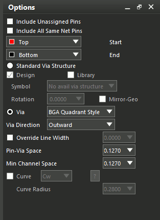
Step 9: The Options panel changes to show numerous settings to create a fanout. Select Outward from the Via Direction dropdown.
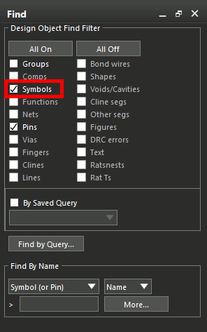
Step 10: Ensure the option for Symbols is checked in the Find panel.
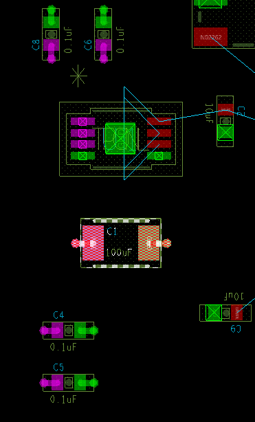
Step 11: Click to select the components with all pins connecting to power and ground to start creating the fanouts. These components are easy to identify because they only have magenta and green pins.
Create Fanouts for Pins in OrCAD PCB
Note: Most surface-mount components have more connections than power and ground. These components require fanouts on individual pins.
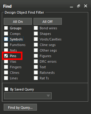
Step 12: Uncheck Symbols in the Find panel. Ensure Pins is checked.
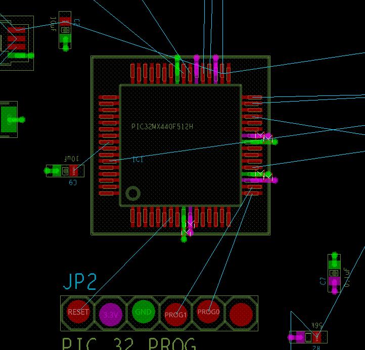
Step 13: Select any remaining power and ground pads on the PCB to create the fanouts.
Note: It is not necessary to select any through-hole pins, they act as vias and connect to the appropriate planes.
Modify Fanouts in OrCAD PCB
Step 14: Creating fanouts on pins that are close together may cause spacing DRC errors. One way to fix this is to move some of the offending nets inside the component. Change the via direction to Inward in the Options panel.
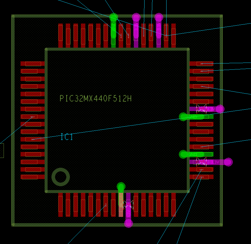
Step 15: Click the affected pins to move the fanouts inward.
Note: Spacing errors remain because the thick traces are too close together.
Step 16: Check Override Line Width in the Options panel.
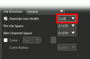
Step 17: Enter a thinner width, such as 0.28, into the Override Line Width field.
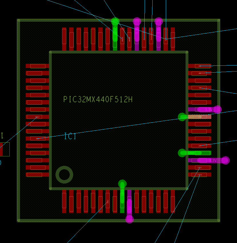
Step 18: Click the pins to adjust the trace width of the fanouts and clear the errors. Right-click and select Done when finished. The fanouts have been created and all power and ground pins have been connected to the appropriate planes.
Wrap Up & Next Steps
Quickly and easily create fanouts to connect surface mount components to power and ground, enhance routing flexibility and improve manufacturability with OrCAD PCB Designer.
Test this feature and more with a free trial of OrCAD. Get more how-tos for OrCAD at EMA Academy.
