Modern electronics could not exist without semiconductors and digital electronics but as electronics become faster and more complex, it’s essential to model realistic behavior to ensure design accuracy. At high speeds, digital electronics are susceptible to issues with propagation delay, and any stray capacitance present on the board could lead to attenuation, which could prevent a high input from ever reaching the device’s threshold voltage. PSpice allows you to quickly create custom Buffer and Inverter SPICE models for accurate simulation of digital designs with a wizard-based approach.
This quick how-to will provide step-by-step instructions on how to create accurate buffer and inverter SPICE models with the Modeling Application in OrCAD PSpice.
To follow along, download the materials provided above the table of contents.
How-To Video
 Open in New Window
Creating Buffer and Inverter SPICE Models
Step 1: Open the provided design in OrCAD PSpice 23.1.
Note: A wizard-based approach to digital models is new in version 23.1. See other new features here.
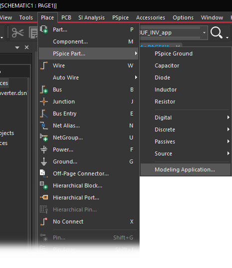
Step 2: Select Place > PSpice Part > Modeling Application from the menu.
Step 3: In the Modeling Application, expand Digital > Gates.
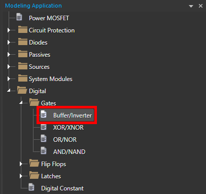
Step 4: Select Buffer/Inverter.
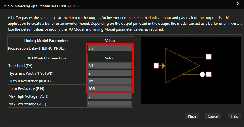
Step 5: The Buffer/Inverter options window opens. Enter the following model parameters:
- Propagation Delay: 6n
- Threshold: 2.4
- Hysteresis Width: 2
- Output Resistance: 1m
- Input Resistance: 10G
Note: The logic device being modeled has negligible output resistance and requires negligible input current. Learn how to identify these parameters from device datasheets to create a realistic representation of buffers and inverters here.
Step 6: Click Place.
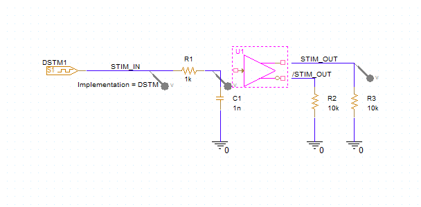
Step 7: Click to place the inverter/buffer assembly in the schematic.
Note: This symbol has a non-inverting and inverting output to simulate a buffer and inverter circuit block.
Step 8: Select Place > Wire from the menu, the Wire button from the toolbar, or press W on the keyboard.
Step 9: Click to make the following connections:
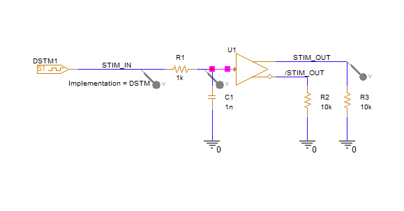
- The buffer input to the RC filter output
- The non-inverting output to net STIM_OUT
- The inverting output to net /STIM_OUT
Step 10: Press Escape on the keyboard when finished.
Note: These nets are drawn to line up with their respective connections on the buffer.
Running the Simulation
Step 11: Select PSpice > Run from the menu.
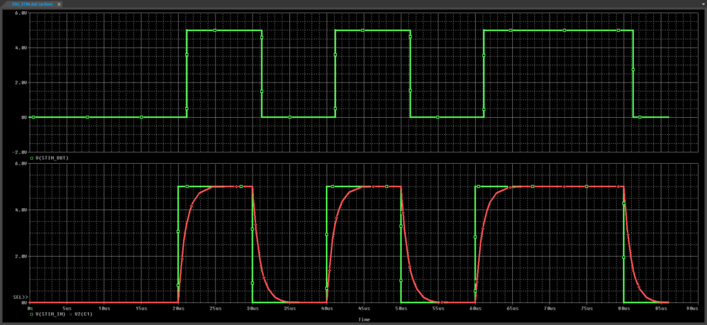
Step 12: View the results. The RC filter and hysteresis delay the output slightly.
Modifying the Circuit
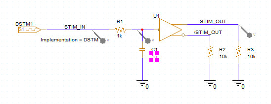
Step 13: Back in the schematic, double-click the value for C1 to change it.
Step 14: Enter 22p for the value and click OK.
Step 15: Select PSpice > Run from the menu.
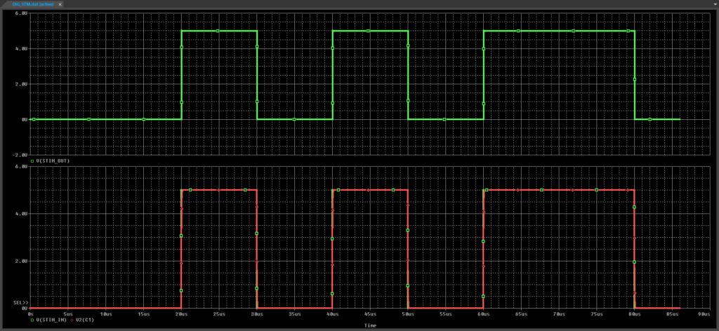
Step 16: View the results. The delay is improved and the output matches the input closely.
Viewing the Inverted Output
Step 17: Double-click V(STIM_OUT) in the legend to change the trace formula.
Step 18: Enter V(/STIM_OUT) in the Trace Expression field to change to the inverted output. Click OK.
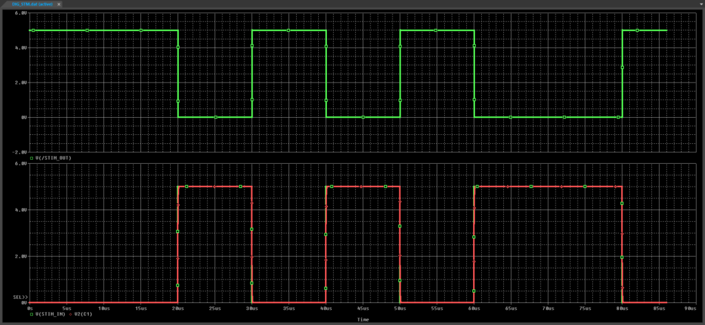
Step 19: View the results. The inverted output is shown.
Wrap Up & Next Steps
Quickly create the required buffer and inverter SPICE models and simulate accurate digital circuit behavior with the PSpice Modeling Application in OrCAD PSpice. Upgrade to the latest 23.1 release or test out this feature and more with a free trial of OrCAD.

