As electronic designs get smaller and more complex, simulation to ensure a device functions as intended has become much more critical. But even if a design performs well in schematic simulation, how it performs on the PCB is another matter altogether. Impedance mismatches, thin traces, and a lack of shielding can create problems that may not be apparent until the board is already in production. New in OrCAD X Presto 24.1 the ability to create and analyze a topology during the PCB layout to determine critical rules, improve signal integrity, and identify issues before production, potentially averting costly respins.
This quick how-to will provide step-by-step instructions on how to create and analyze a topology for critical nets in OrCAD X Presto.
To follow along, download the provided files above the table of contents.
How-To Video
 Open in New Window
Activating the Constraint Manager
Step 1: Open the provided design in OrCAD X Presto.
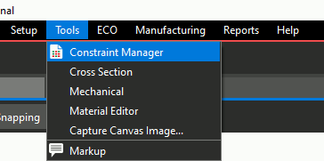
Step 2: Select Tools > Constraint Manager from the menu.
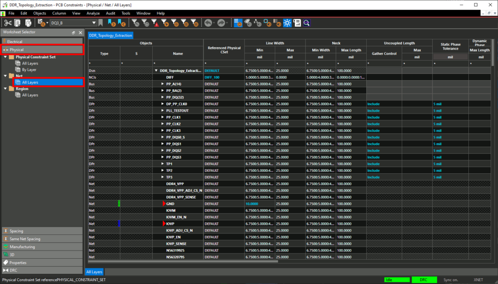
Step 3: The Constraint Manager opens. Select the Physical domain from the Worksheet Selector.
Step 4: Select the Net > All Layers worksheet. The table is populated with all nets in the design and the physical constraints assigned to them.
Activating Topology Explorer

Step 5: Expand bus PP_DQ(32) and select net PP_DQ<30> in the table.
Step 6: Select Tools > Explore Topology from the menu.
Step 7: Topology Workbench opens to two topologies- one for the net itself and one for the electrical constraint set assigned to the net. Select the tab for pp_dq_30 to view the net topology.
Note: The generated topologies are included in a subfolder with the net name in the working directory.
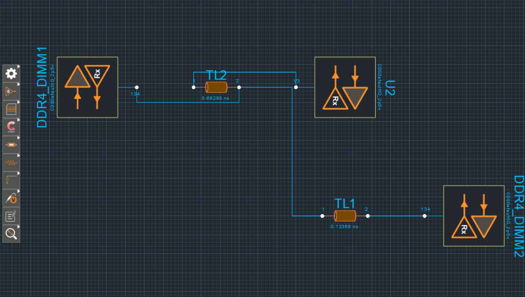
Step 8: View the topology. IO blocks corresponding to DDR4_DIMM1, DDR4_DIMM2, and U2 are shown, connected by transmission lines.
Preparing the Topology for Simulation
Step 9: To perform transient analysis on the net topology, one of the IO blocks must be classified as a transmitter. Select the block for DDR_DIMM1.
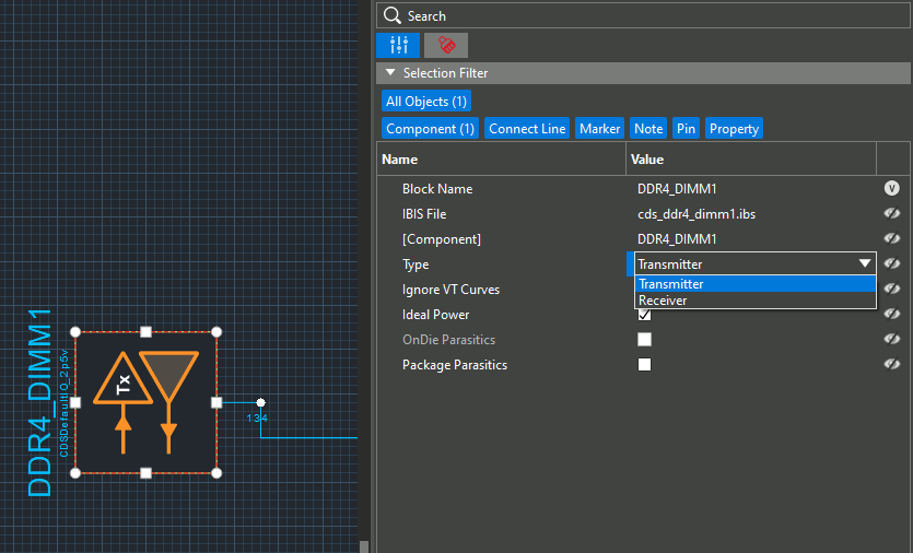
Step 10: In the Properties panel, select Transmitter from the Type dropdown. The block updates to show Tx.
Step 11: Select Set Analysis Options from the workflow.
Step 12: The Analysis Options panel opens at the bottom of the window. Select the IO Models and Stimulus Tab and DDR4_DIMM1 under Model Selection.

Step 13: In the Model Selection table, double-click each cell for Signal to configure the simulation options as follows:
- Data Rate: 0.05
- # of Bits: 4
- Stimulus Pattern: 0101
- Stimulus Offset: 1
Step 14: Close the Analysis Options panel.
Analyze a Topology in OrCAD X Presto
Step 15: In the Topology Explorer workflow, select Start Transient Analysis to run the analysis.
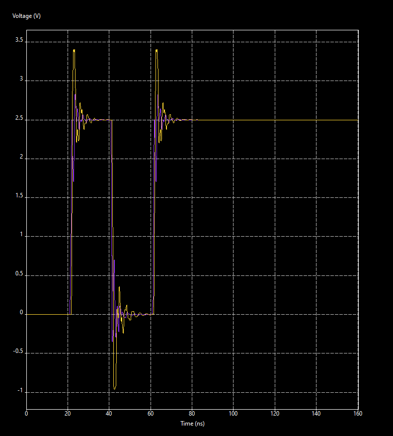
Step 16: The 2D Curves tab opens. View the results. The data pulses at both receiver models are shown.
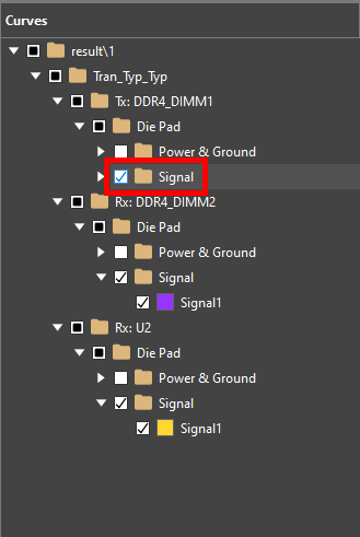
Step 17: In the Curves list, expand Tx: DDR4_DIMM1 > Die Pad and check Signal to view the transmitted signal.
Note: Double-click the color box for the signal to change its plot color.
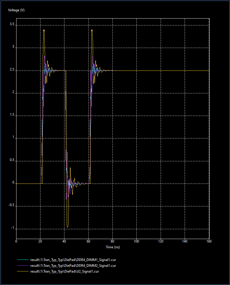
Step 18: View the curves plot again. The transmitter curve is plotted with the receiver curves. The receiver curve for U2 indicates significant overshoot from reflections.
Step 19: Close the 2D Curves tab.
Note: With the topology extracted, parameters can be modified to determine the ideal configuration for signal performance and the associated design rules.
The overshoot shown can be corrected by impedance matching on the PCB. To learn more about correcting overshoot, take our free workshop here.
Wrap Up & Next Steps
Quickly create and analyze a topology in OrCAD X Presto to enhance performance of critical nets, determine the necessary design rules, and identify potential issues to improve signal integrity in your PCB designs. Test out this feature and more with a free trial of OrCAD X. For more how-tos and step-by-step walkthroughs, visit EMA Academy.