With today’s ever-changing design landscape, new components are introduced almost every day. Manually drawing each required part for your PCB designs is tedious and time-consuming. With EDABuilder, you can quickly and easily create a schematic symbol directly from the datasheet for accurate component modeling in a fraction of the time.
This quick how-to will provide step-by-step instructions on how to create a schematic symbol from a component datasheet with EDABuilder.
To follow along, download the provided files above the table of contents.
How-To Video
 Open in New Window
Loading a PDF
Step 1: Open EDABuilder.
Step 2: Select File > New > Symbol from PDF from the menu.
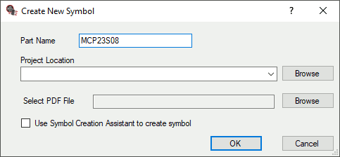
Step 3: The Create New Symbol window opens. Enter MCP23S08 for the Part Name.
Step 4: Select Browse for the Project Location.
Step 5: Select the working directory and click OK.
Step 6: Select Browse for Select PDF File.
Step 7: Browse to the provided pdf file. Select the file and click Open. Click OK to create the project file.
Extract Pin Information from a Component Datasheet
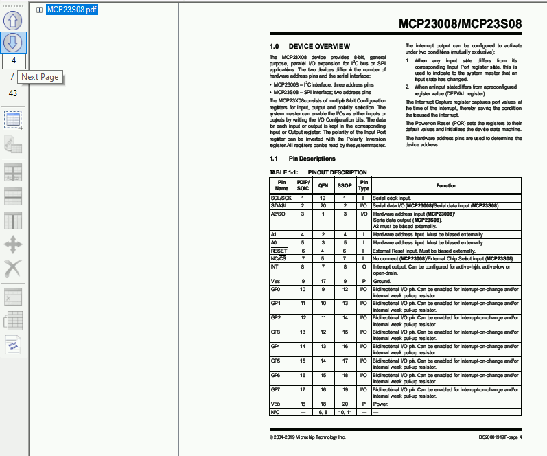
Step 8: The EDABuilder canvas opens to show the loaded PDF. Select the Next Page button three times to navigate to page 4 of the datasheet.
Note: Scroll up and down to zoom in and out as needed.
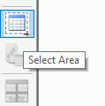
Step 9: Choose the Select Area tool from the sidebar.
Step 10: The Select Area window opens. Select Table/Pin Out Diagram and click OK.
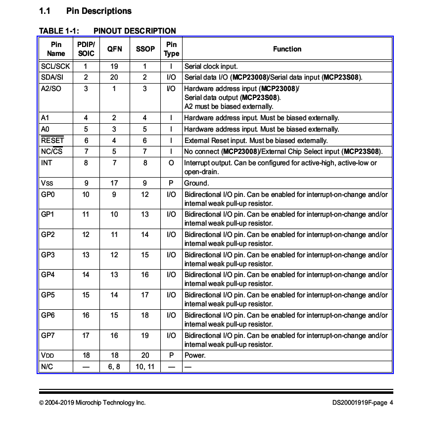
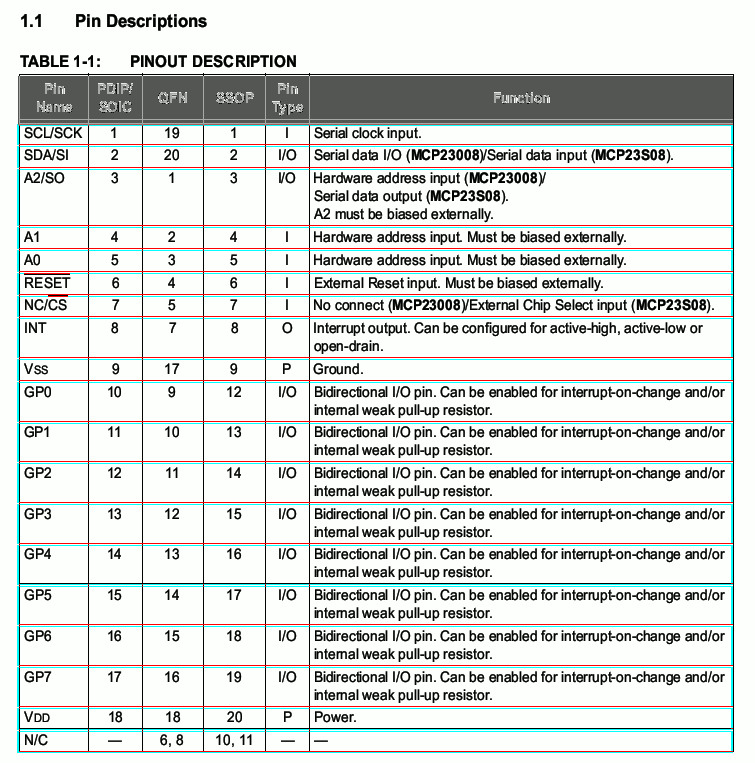
Step 11: Click and drag to select Table 1-1 in the PDF.
A blue grid is generated over the table and the table text is listed in the Data Preview panel.
Note: For more information on how to import a table from a PDF, see our how-to here.
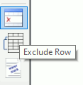
Step 12: Select Exclude Rows from the sidebar.
Step 13: Select the column header of the table and the empty row underneath it to exclude them from the final pin function table.
Modify Component Data
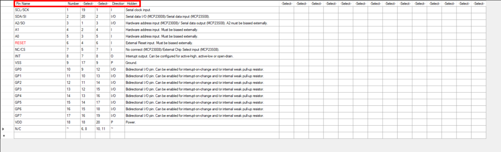
Step 14: Right-click in the canvas and select Extract Data > Extract and Switch to Scratchpad. The Scratchpad canvas opens to the generated table. Table column functions can be configured here.
Note: RESET is highlighted in red, indicating that it was flagged with an inversion bar in the PDF. This will be corrected in the following steps.
Step 15: Click Select in the column header for the pin name column to define the column function.
Step 16: Select Pin Name from the resulting dropdown.
Step 17: Click Select in the column header for the first pin number column. Select Number from the dropdown.
Note: The next two columns can be ignored as these are additional pin numbers given for other packages for the chip.
Step 18: Click Select in the column header for the direction column. Select Direction from the dropdown.
Step 19: Click Select in the column header for the description column. Select Hidden from the dropdown. This will discard the column data when the Capture part is created.
Negate Pins
Step 20: Pins with an inversion bar are highlighted in red. This can be corrected by negating the pins. Select Edit > Negate Pin from the menu.
Step 21: The Map Negation Code window opens. Confirm that only the RESET pin is selected.
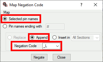
Step 22: In the Map Negation Code window, set the following information:
- Map: Selected Pin Names
- Action: Append
- Negation code: _L
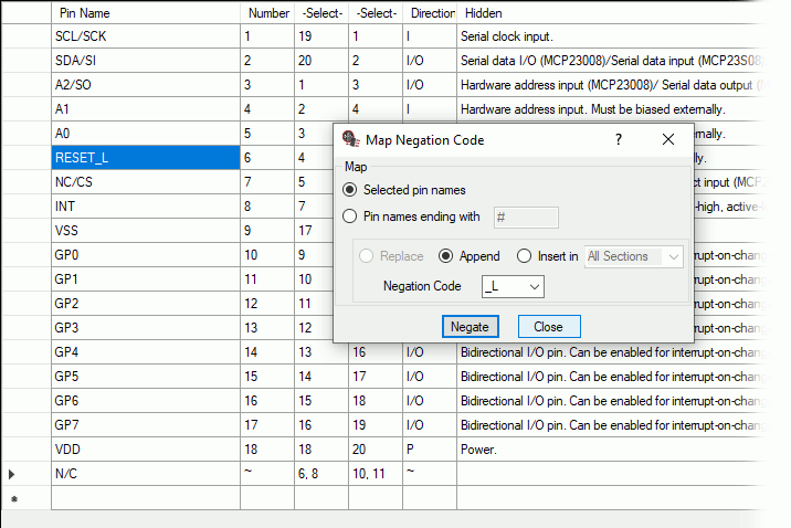
Step 23: Click Negate and Close. “_L” is added to the end of the pin name.
Step 24: Right-click in the canvas and select Copy Data to Symbol View > Copy and Switch to Symbol View to create the symbol.
Identify and Correct Symbol Errors
Step 25: The Check Form window opens, validating the component data and automatically identify any errors and warnings in the symbol creation. Select the first error.
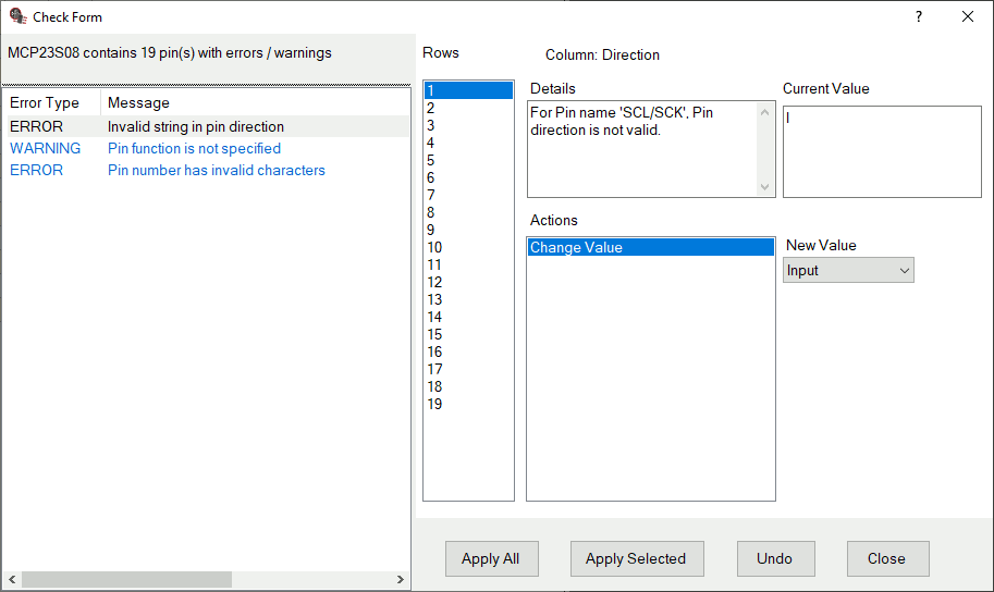
Step 26: Read the error details. This error indicates “invalid string in pin direction.” The format used in the datasheet does not match that required by Capture.
Step 27: Select Row 1 under Rows and choose Input for the new value. Click Apply Selected. The pin direction is changed to the correct Input.
Step 28: Repeat step 27 for each pin/row as follows:
- Row 2: Bidir
- Row 3: Bidir
- Row 4: Input
- Row 5: Input
- Row 6: Input
- Row 7: Input
- Row 8: Output
- Row 9: Ground
- Row 10: Bidir
- Row 11: Bidir
- Row 12: Bidir
- Row 13: Bidir
- Row 14: Bidir
- Row 15: Bidir
- Row 16: Bidir
- Row 17: Bidir
- Row 18: Power
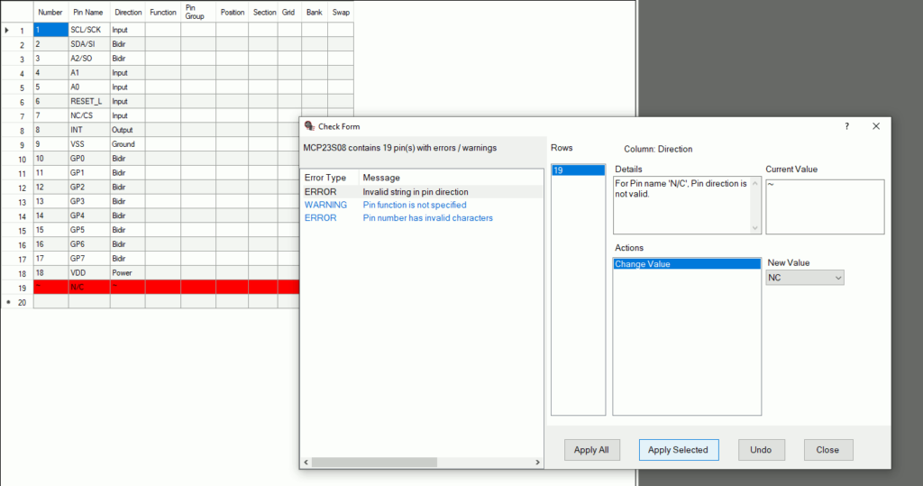
- Row 19: NC
Note: When selecting a row, the pin type may be automatically detected and configured in the Check Form window.
Step 29: Select the next error, which is a warning. The pin function for row 6 is not specified.
Step 30: For Row 6, select Change Value under Actions. Set the New Value to Negative and click Apply Selected.
Step 31: The last error details invalid characters (~) in row 9. Select Replace Invalid Characters with Underscore and click Apply Selected.
Note: If a prompt appears that all errors have been cleared, click OK.
Manually Create a Schematic Symbol Graphic
Note: There are multiple methods to create a schematic symbol graphic in EDABuilder. These steps will cover the manual methods including assignment of pins and a drag-and-drop approach.
Step 32: Right-click in the canvas and select Edit Symbol Graphics. The Symbol View subpanel opens.
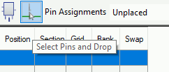
Step 33: Choose Select Pins and Drop from the toolbar to activate the click-and-drop mode.
Step 34: Select pin 1 from the table and click the left edge of the symbol to place the pin. Pin 1, with name SCL/SCK, is placed and the next pin is automatically selected in the table.
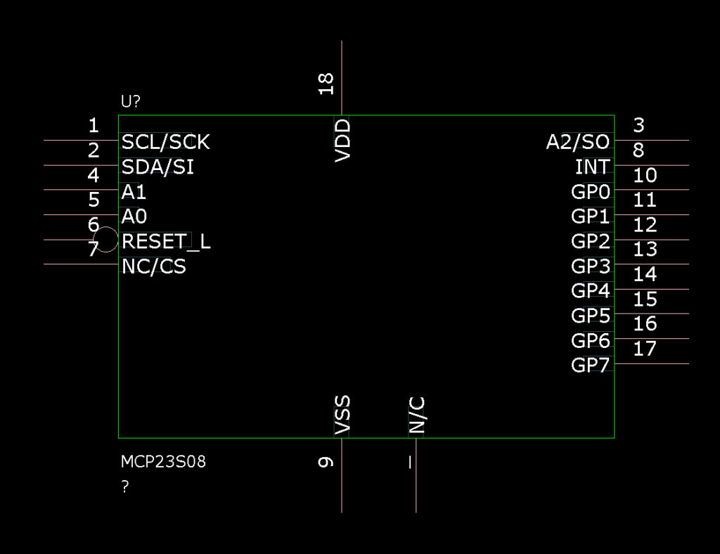
Step 35: Select the following pins in the pin table then click each side of the symbol as defined to place the pins:
- Left: 2, 4-7
- Right: 3, 8, 10-17
- Top: 18
- Bottom: 9, NC
Note: Highlight a group of nets in the pin table to place several pins on the schematic symbol at once.
Step 36: Pins can also be assigned automatically based on rules. To assign pins this way, the symbol must first be cleared. Right-click in the table and select Unassign All.
Automatically Create a Schematic Symbol Graphic
Note: With EDABuilder you can automatically assign and place pins on the schematic symbol based on rules.
Step 37: Right-click and select Auto Assign by Rules to automatically assign pin positions by rule.
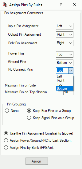
Step 38: The Assign Pins By Rules window opens. Set the Input Pin Assignment to Left, the Output Pin Assignment to Right, and the Bidir Pin Assignment to Right.
Step 39: Set the Power Pins assignment to Top and the Ground Pins assignment to Bottom. Set the No Connect Pins assignment to Bottom.
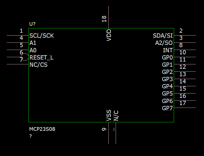
Step 40: Click Assign. The pins are added to the symbol automatically. An inverting bubble is added to RESET.
Exporting the Symbol
Step 41: To export an OrCAD Capture symbol from EDABuilder, select File > Export > OrCAD Capture Symbols from the menu.
Step 42: A prompt appears to save the project. Click Yes.
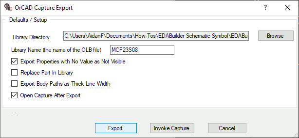
Step 43: The OrCAD Capture Export window opens. Select Browse to choose where to save the library.
Step 44: Browse to the working directory. Select the desired folder and click OK.
Step 45: Enter the name MCP23S08 under Library Name.
Step 46: Check the option for Open Capture After Export and click Export. The file is exported.
Step 47: The Capture CIS Product Choices window opens. Select the appropriate license and click OK.
Viewing the Symbol
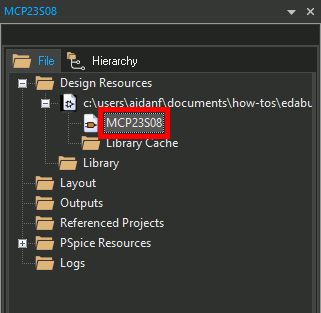
Step 48: Capture opens with the symbol listed in the Project Manager automatically. Double-click the symbol to open the Part Editor.
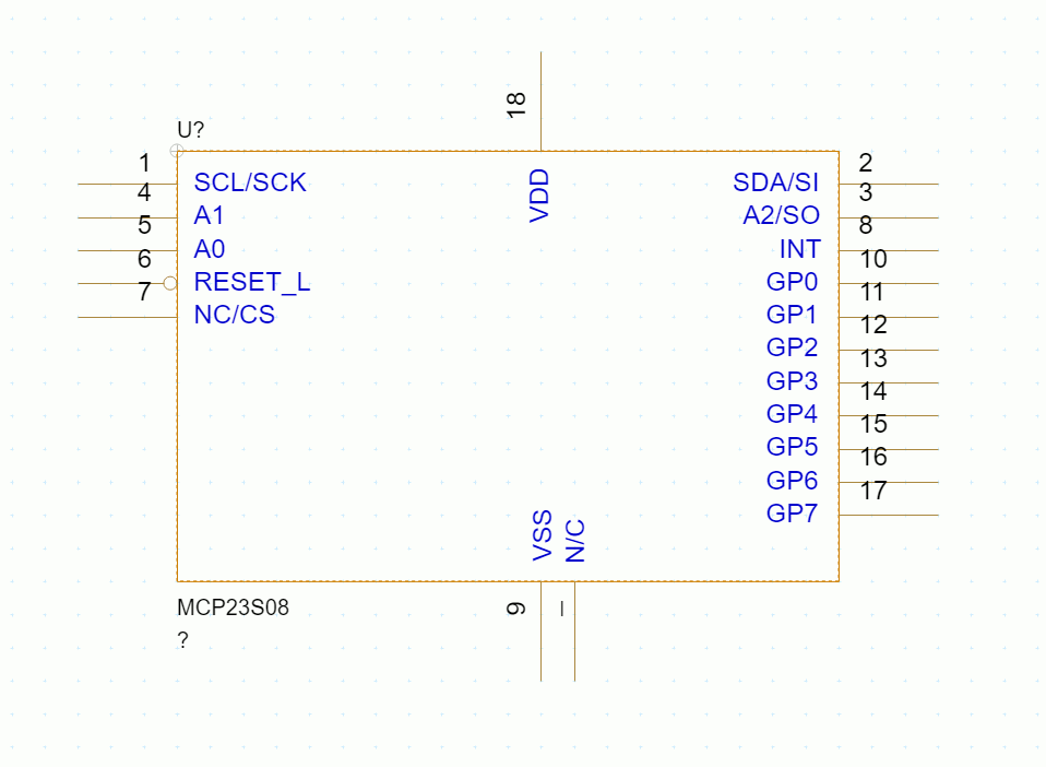
Step 49: The Part Editor opens in OrCAD Capture, showing the completed part. The part can now be used in future designs.
Wrap Up & Next Steps
Efficiently create a schematic symbol with EDABuilder to quickly and accurately model the components required in your schematic design. Get more step-by-step instructions for EDABuilder at EMA Academy.

