Creating PCB footprints and ensuring the pin information matches the schematic symbol can be time consuming, especially as component complexity increases; however, component models are the basis for your PCB designs and any errors can be detrimental to electronic functionality. EDABuilder provides easy-to-use templates, a calculator-based GUI for efficient modification, and automated checks to create a PCB footprint quickly and accurately.
This quick how-to will provide step-by-step instructions on how to create a PCB footprint with EDABuilder.
To follow along, download the provided files above the table of contents.
How-To Video
 Open in New Window
Open a Schematic Part in EDABuilder
Step 1: Open EDABuilder and select File > Open > Part.
Note: A footprint can be created without the corresponding symbol; however, it is recommended to link and verify the schematic symbol and footprint to ensure accuracy. Need help creating a symbol with EDABuilder? Check out our how-to here.
Step 2: Select Browse. Browse to the location of the provided part and select OK.
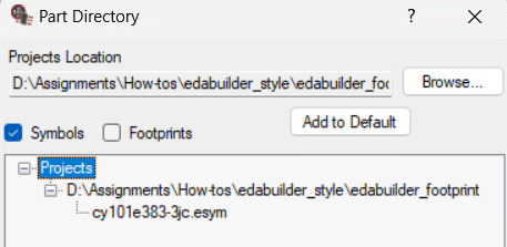
Step 3: Expand the project hierarchy and select the part, cy101e383-3jc. View the schematic symbol.
Create a PCB Footprint in EDABuilder
Step 4: Select File > New > Footprint.
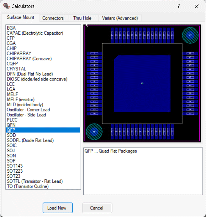
Step 5: Select QFP from the list of available calculators and choose Load New.
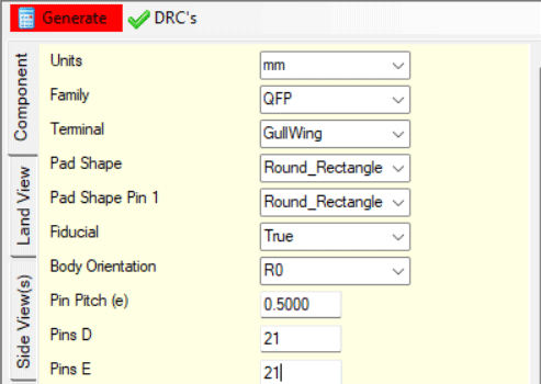
Step 6: View the window. A preview of the footprint is located on the right of the canvas and an interactive, calculator-based GUI is located on the left of the canvas. In the Pins D and Pins E fields, enter 21.
Step 7: The Generate button at the top of the calculator turns red, indicating there has been a change that needs to be reflected in the PCB footprint. Select Generate.
Step 8: A prompt will appear that the update will cause an error. This is because we haven’t updated the dimension values yet. Click OK and view the updated preview. The number of pins on each side of the PCB footprint is now 21 instead of 16.
Modify the PCB Footprint
Note: Reference the part datasheet to verify and modify the dimensions of the PCB footprint to reflect the component packaging. The datasheet for this component has been included in the provided files.
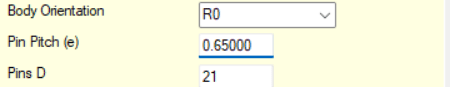
Step 9: The PCB footprint includes critical dimensions required for accurate footprint creation. These dimensions can be updated in the calculator. Set the Pin pitch (e) to 0.65.
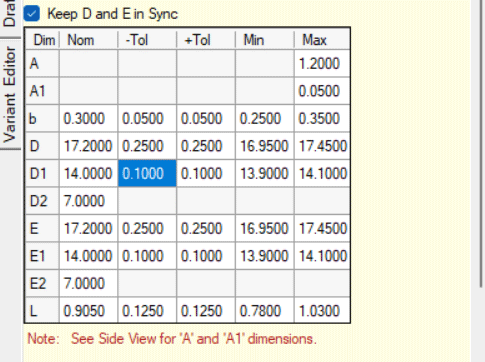
Step 10: In the table, locate b and enter a nominal (nom) value of 0.3.
Step 11: In the table, locate D. Enter a nominal (nom) value of 17.2 and a tolerance of 0.25.
Note: The value of E is updated automatically since the box Keep D and E in sync is checked.
Step 12: In the table, locate D1. Enter a nominal (nom) value of 14 and a tolerance of 0.1.
Step 14: Select Generate.
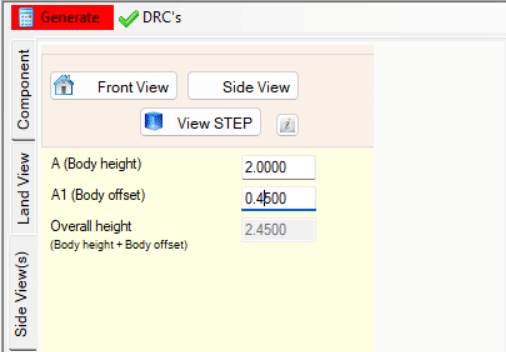
Step 15: Select the Side View(s) tab in the calculator form.
Step 16: Enter 2 for the A (Body Height).
Step 17: Enter 0.45 for the A1 (Body Offset).
Step 18: Select Generate.
Step 19: Select the Component tab in the calculator form.
Annotate the PCB Footprint
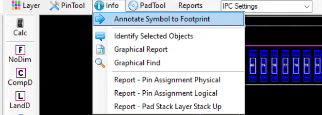
Step 20: Select Info > Annotate Symbol to Footprint.
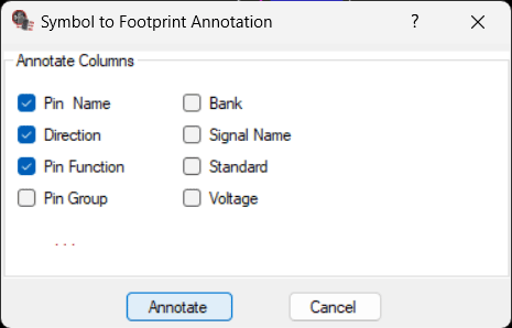
Step 21: Select the columns to annotate from the schematic to the footprint. For this example, select the following:
- Pin Name
- Direction
- Pin Function
Step 22: Select Annotate.
Perform Component Checks

Step 23: Select Reports > Footprint to Symbol Compare.
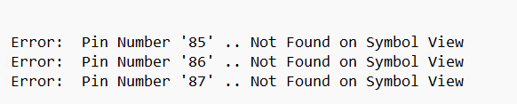
Step 24: View the report. Pins 85, 86, and 87 are not found in the symbol. In the PCB footprint these pins are the fiducials and thermal pad.
Step 25: Close the report.

Step 26: In the calculator, uncheck the box for Thermal Pad to remove the thermal pad from the footprint.
Step 27: Under the Fiducial dropdown, select False.
Step 28: Select Generate.
Step 29: A prompt will appear that variance was detected. Select Go.
Linking a Schematic Symbol and PCB Footprint with EDABuilder
Note: Linking a schematic symbol and PCB footprint automatically creates the relationship upon export.
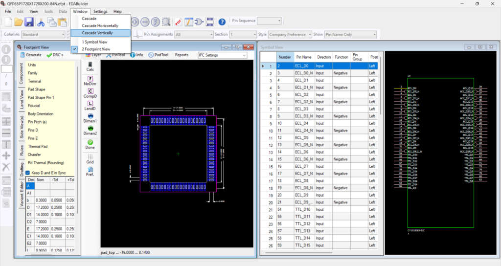
Step 30: Select Cascade > Vertical from the menu to view both the symbol and footprint.
Step 31: Select the symbol view then select Data > Add Footprint.
Step 32: Provide a name for the footprint, browse to the project location if needed and select OK.
Export a PCB Footprint with EDABuilder
Step 33: Select the footprint view then select File > Export > OrCAD PCB/ Allegro Export.
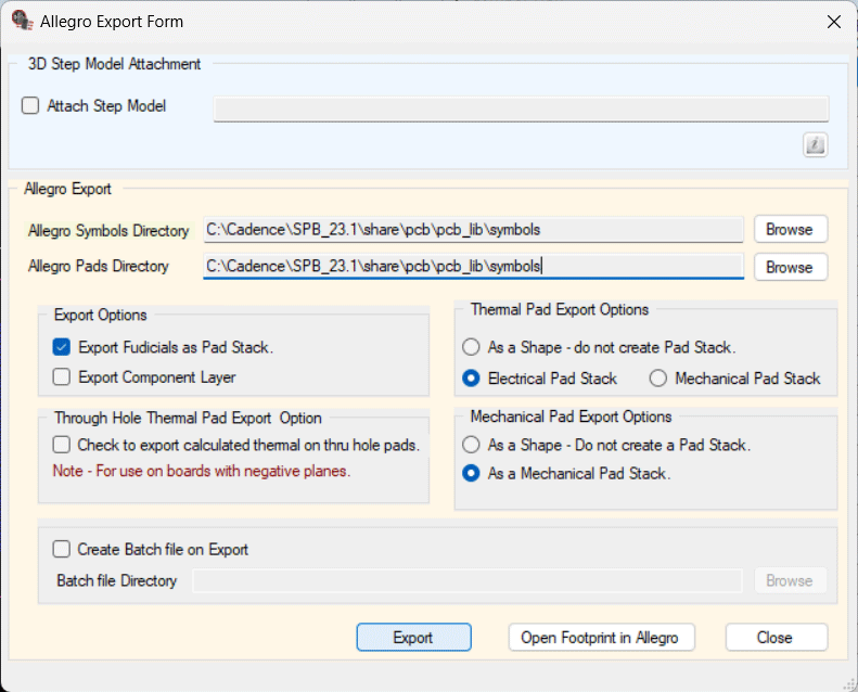
Step 34: Browse to set the desired directory for the Allegro Symbols and Allegro Pads.
Note: In the export window you can also configure the following:
- Mapping a STEP file to the PCB footprint
- Thermal pad export settings
- Mechanical pad export settings
- Create a batch file on export
- Export Component Layer
- Export Fiducials as Pad stacks
Learn how to generate a 3D STEP model with EDABuilder here.
Step 35: Select Export.
Step 36: The Cadence Product Choices window will open. Select the desired software and click OK to generate the footprint.
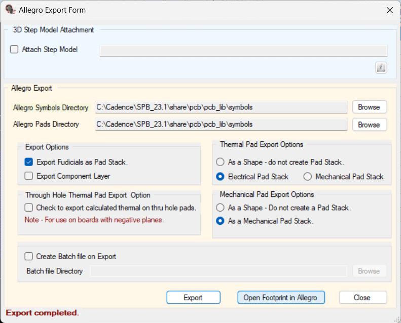
Step 37: When export is complete select Open Footprint in Allegro.
Step 38: The Cadence Product Choices window will open. Select the desired software and click OK to view the footprint.
Wrap Up & Next Steps
Quickly create a PCB footprint using EDABuilder with easy-to-use templates, a calculator-based GUI for efficient modification, and automated checks to accelerate your product development process. Get more step-by-step instructions for EDABuilder at EMA Academy.

