Many times, manufacturers provide simulation models to realistically analyze circuit behavior; however, the corresponding schematic symbol isn’t always provided. To ensure clear and efficient communication of the components in the design, sometimes schematic symbols need to be created. Easily create schematic symbols and link SPICE models in OrCAD.
This how-to will provide step-by-step instructions to import simulation models and create schematic symbols in PSpice Designer.
To follow along with this tutorial, download the provided files above the table of contents.
How-To Video
Renaming a Model File
Step 1: Right-click on the MCP6547.txt file from the provided files and select Rename.
Note: May manufacturers often provide models in .txt format. This process can be completed for any simulation model in text format.
Step 2: Change the extension to .lib.
Note: The extension must be written in lowercase letters to be able to run in PSpice. PSpice will not recognize .LIB.
Creating a New Library
Step 3: Open the provided design, SineAmp2.dsn, in OrCAD PSpice Designer.
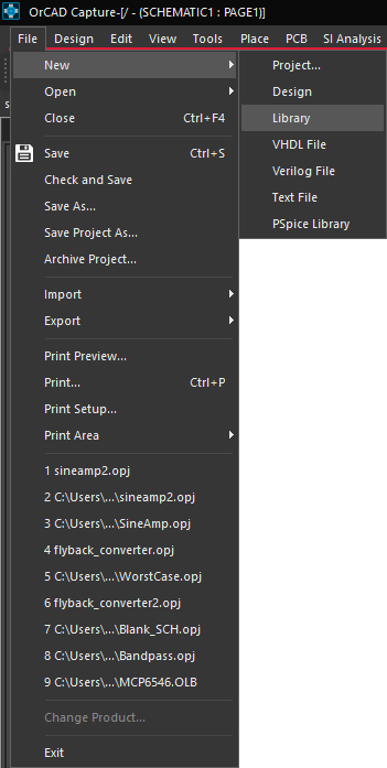
Step 4: Select File > New > Library from the menu.
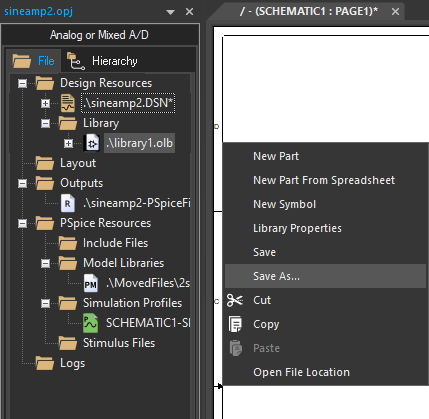
Step 5: A new library has been added under Library in the project hierarchy. Right-click and select Save As.
Step 6: Browse to a location to save the library. Save the library as MCP6546.OLB.
Create Schematic Symbols
Step 7: Right-click on the library and select New Part.
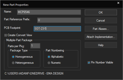
Step 8: Name the part MCP6546. Set the PCB footprint to SOT-23-5.
Step 9: Leave all other settings as the defaults and click OK.
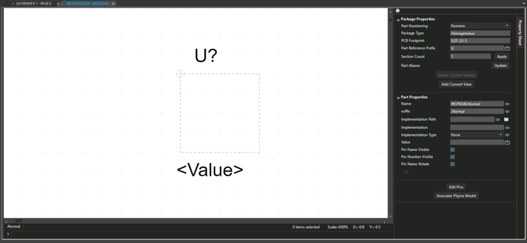
Step 10: Adjust the size of the bounding box to be 4 units wide and 4 units tall by dragging the corners of the box.
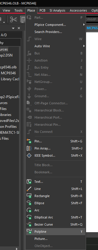
Step 11: Select Place > Polyline from the menu or click the Place Polyline button on the toolbar.
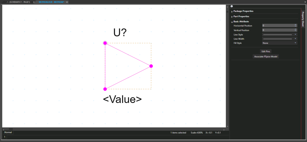
Step 12: Click to begin a line and click to end the line to draw the triangular shape as shown above. Right-click and select End Mode when finished.
Note: Hold down the Shift key on the keyboard to draw a diagonal line.
Step 13: Select Place > Line from the menu or click the Place Line button on the toolbar.
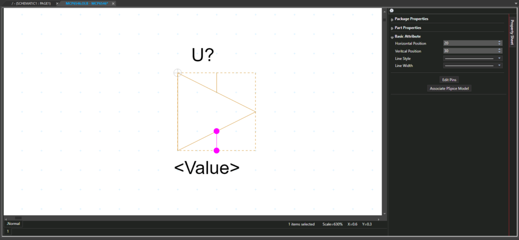
Step 14: Draw two lines for voltage supply extending from the triangle midpoints. Right-click and select End Mode when finished.
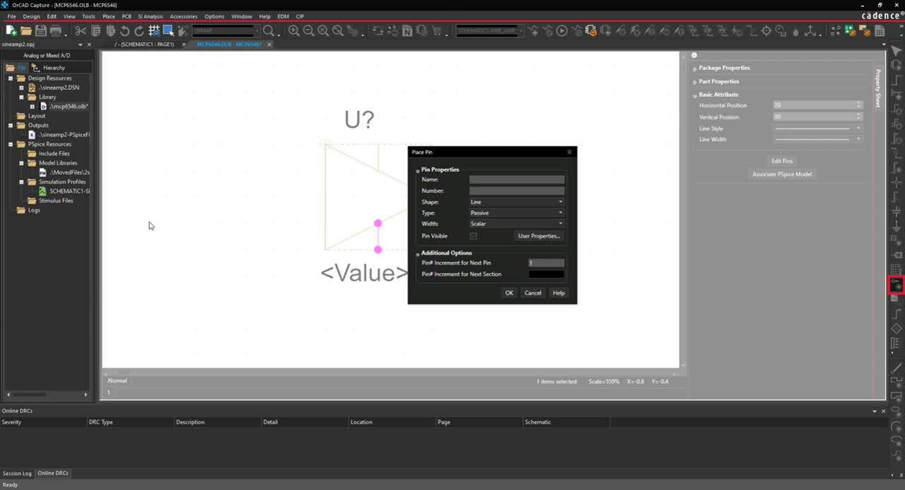
Step 15: Select Place > Pin from the menu or click the Place Pin button on the toolbar.
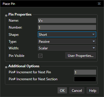
Step 16: Set the name to V+ and number to 1. Set the shape to Short. Click OK.
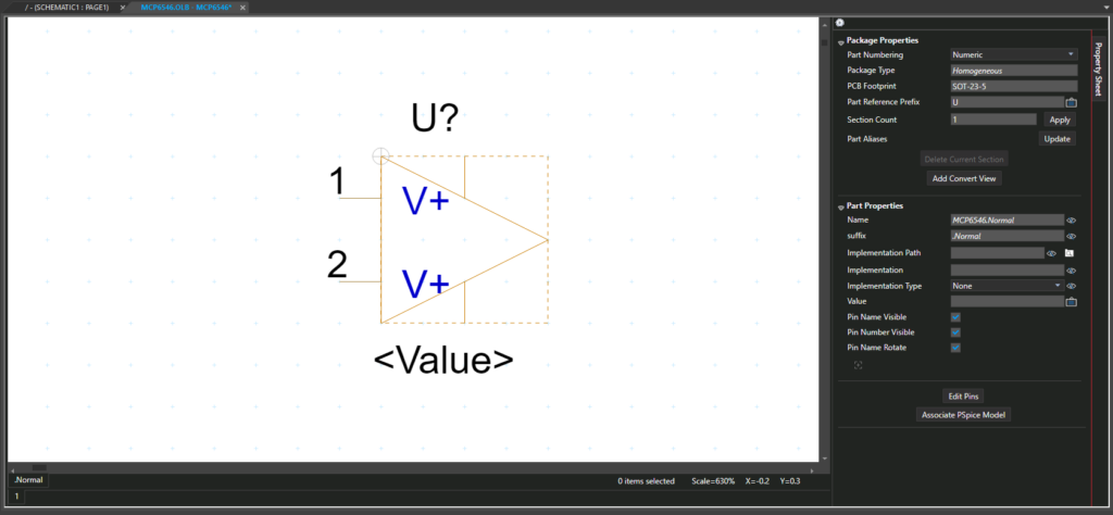
Step 17: Click to place a pin at the top-left of the triangle and another at the bottom-left.
Step 18: Click to place the positive and negative supply pins at the top and bottom.
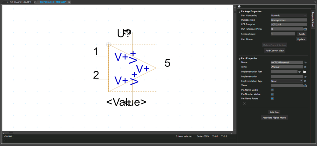
Step 19: Click to place the output pin. Right-click and select End Mode.
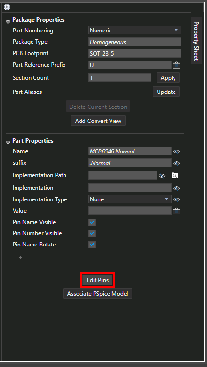
Step 20: Select the Edit Pins button from the sidebar. The Edit Pins window will open.
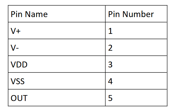
Step 21: Set the pin names to match the following table:
Step 22: Click OK.
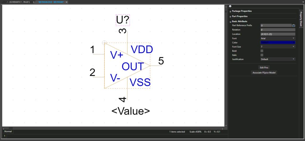
Step 23: On the part canvas, click and drag the VDD, VSS, U?, and <Value> labels away from the component for better visibility. Rotate as needed with R on the keyboard.
Step 24: Select File > Save to save the part.
Linking a PSpice Model
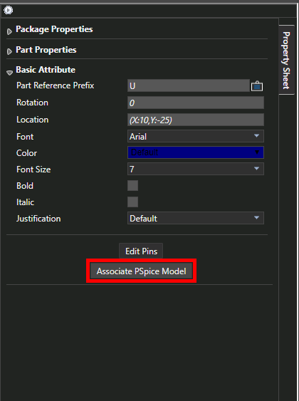
Step 25: Select Associate PSpice Model.
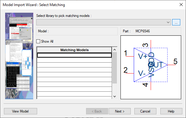
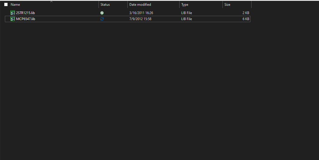
Step 26: Under Select library to pick matching models, select the ellipsis. Browse to the location of the MCP6547.lib file and select Open.
Step 27: Select Next.
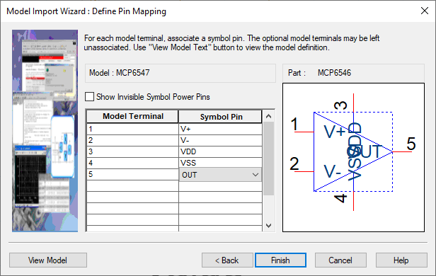
Step 28: Set the symbol pins to match the model terminals in the table.
Step 29: Click Finish.
Step 30: Select File > Save to save the part and close the tab.
Creating the Schematic
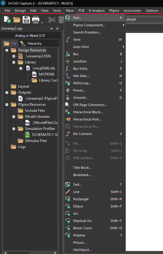
Step 31: Select Place > Part from the menu or click the Place Part button on the toolbar.
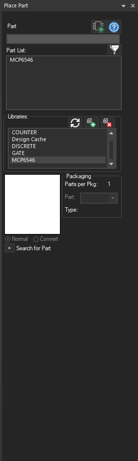
Step 32: In the Libraries table, select MCP6546. The newly created part will appear in the Part List.
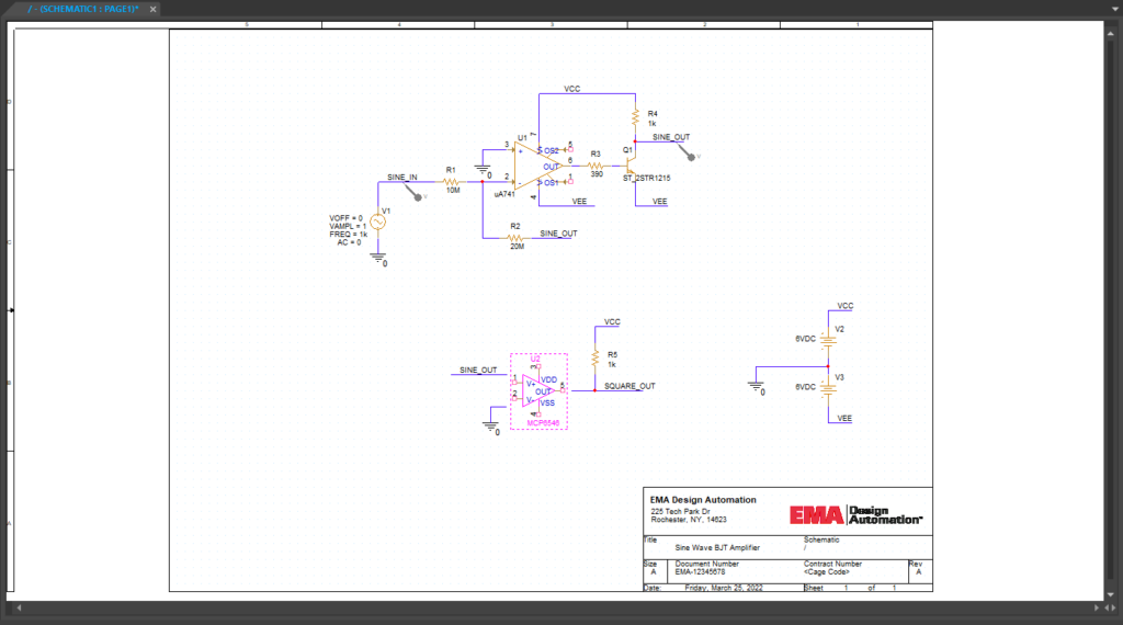
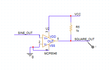
Step 33: Select the existing op-amp, U2, and press Delete on the keyboard.
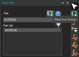
Step 34: In the Place Part Window, select the part and click Place Part.
Step 35: Click to place the part in the schematic canvas. Right-click and select End Mode.
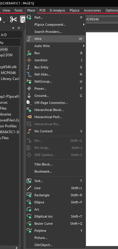
Step 36: Select Place > Wire from the menu, the Wire button on the toolbar, or press W on the keyboard.
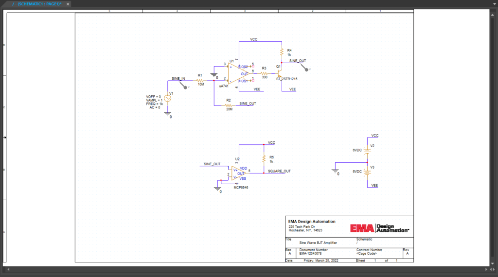
Step 37: Wire the connections to each pin of the comparator. Press Escape on the keyboard when finished.
Performing a Simulation
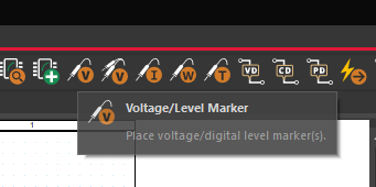
Step 38: Select the Voltage/Level Marker button from the toolbar.
Step 39: Click to place a probe on the SQUARE_OUT net. Right-click and select End Mode.
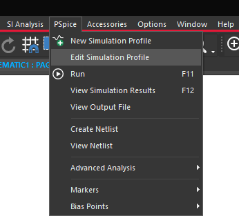
Step 40: Select PSpice > Edit Simulation Profile from the menu.
Step 41: Select Configuration Files from the sidebar.
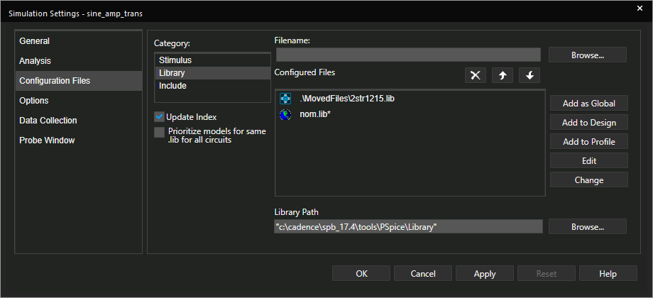
Step 42: Select Library under Category.
Step 43: Select Browse. Navigate to the MCP6547.lib file, select it and click Open.
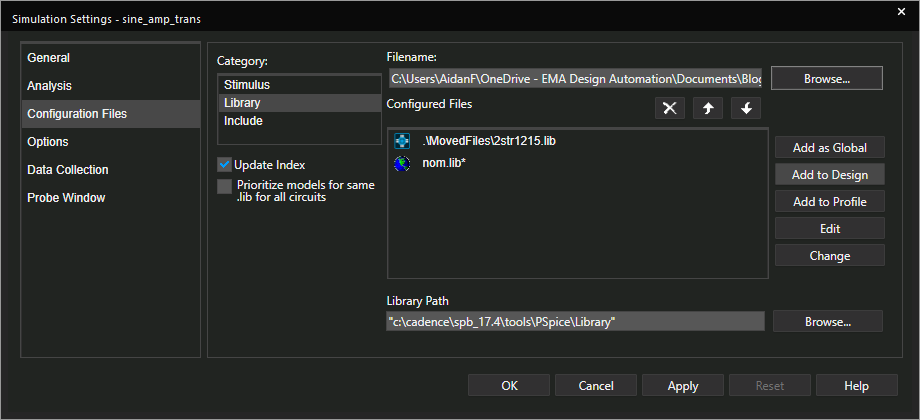
Step 44: Select Add to Design.
Note: If libraries are not configured, the simulation will not run. Select Add to Global to configure the file for all future simulations.
Step 45: Click OK to save the simulation settings and close the window.
Step 46: Select PSpice > Run from the menu.
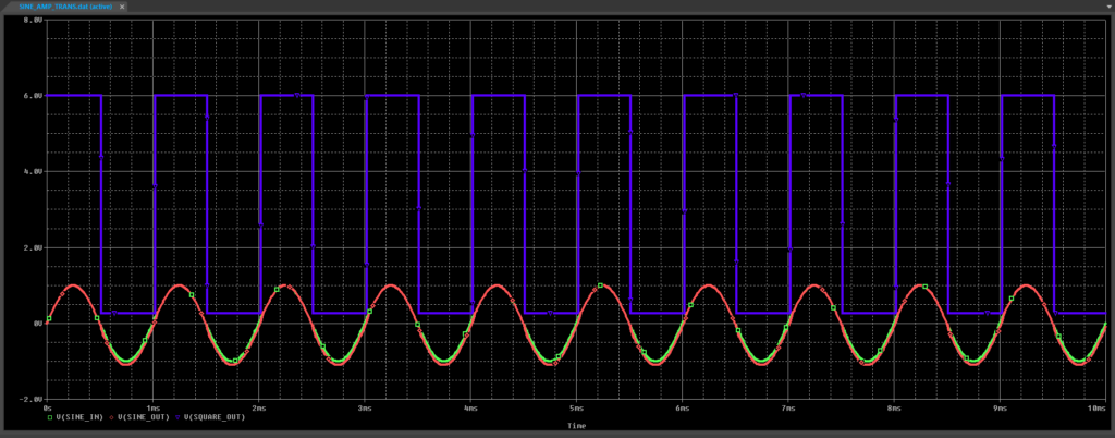
Step 47: View the simulation results.
Wrap up & Next Steps
Easily create schematic symbols and associate manufacturer’s simulation models to clearly communicate design intent with OrCAD PSpice. See how PSpice can validate and optimize your circuit functionality with a free trial.

