With design form factors becoming smaller and more complex, creating an accurate board outline early in the design process is essential. While dimensions and drawings provided by the mechanical engineering team can be used to approximately determine edge and hole locations, it is much easier and less error-prone to create a board outline directly from the CAD file. With OrCAD X PCB Designer, easily create a board outline from a DXF and other mechanical files including:
- DXF
- IDX
- IDF
This quick how-to will provide step-by-step instructions on how to create a board outline from a DXF in OrCAD X PCB Designer.
Need to import a DXF file to create a board outline in OrCAD X Presto? Get the step-by-step instructions here.
To follow along, download the provided files above the table of contents.
How-To Video
 Open in New Window
Creating a Board File
Step 1: Open OrCAD X PCB Designer.
Step 2: Select File > New from the menu.
Step 3: The New Drawing window opens. Select Board for the drawing type and select Browse.
Step 4: Browse for the working directory. Enter DXF_Board for the board name and click Open.
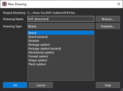
Step 5: Back in the New Drawing window, click OK to create the board file.
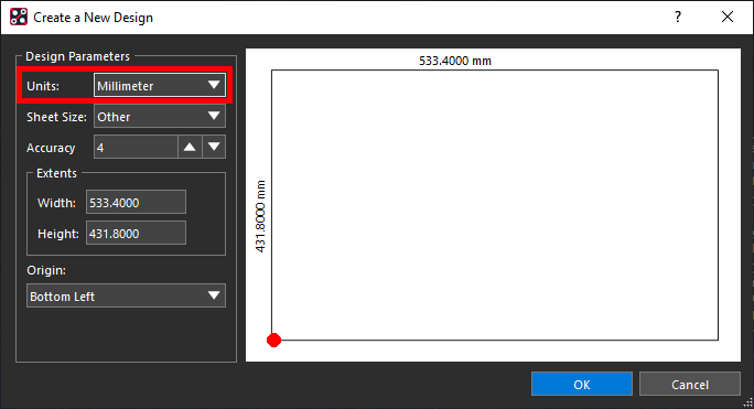
Step 6: The Create a New Design window opens. Set the Units to millimeter and click OK. The board is created.
Creating a New Subclass Layer
Note: To create a board outline from a DXF in OrCAD X, ensure the DXF can be imported onto a layer that will not affect the board outline. A new subclass can be created to import the DXF.
Step 7: Select Setup > More > Subclasses from the menu to open the Define Subclass window.
Step 8: Select the button for Drawing Format.
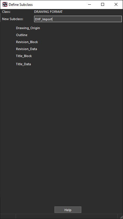
Step 9: In the resulting window, enter DXF_Import as the name and press Enter.
Step 10: Close the window.
Step 11: In the original Define Subclass window, click OK to save the settings and close the window.
Importing the DXF
Step 12: Select Import > MCAD > DXF from the menu.
Note: IDF and IDX files can also be imported through this menu.
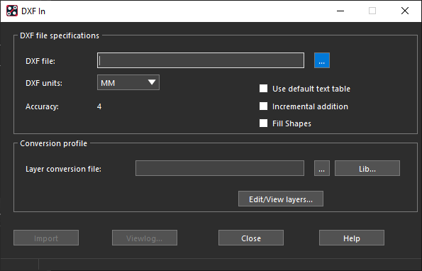
Step 13: The DXF In window opens. From this window, you can select the DXF units and layer conversion file if available. You can also define whether to close filled shapes, clear the current database, and match the imported text. Select the ellipsis for DXF File to load the file.
Step 14: Browse to the provided Special_Outline.dxf file. Select the file and click Open.
Step 15: To create a board outline from a DXF in OrCAD X, a layer conversion file needs to be created. Select Edit/View Layers.
Note: A layer conversion file can also be loaded if the DXF file was created in PCB Designer.
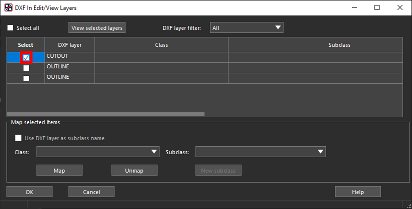
Step 16: The DXF In Edit/View Layers window opens. Check the option under Select for DXF layer Cutout.
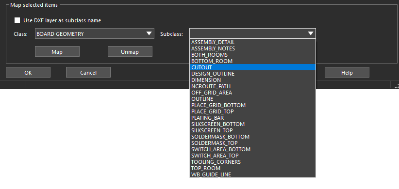
Step 17: Under Map Selected Items, select Board Geometry from the Class drop-down menu and Cutout from the Subclass dropdown.
Note: DXF files will vary. Ensure that the correct layers are mapped based on your PCB and drawing file.
Step 18: Select Map. The class and subclass are mapped to the layer.
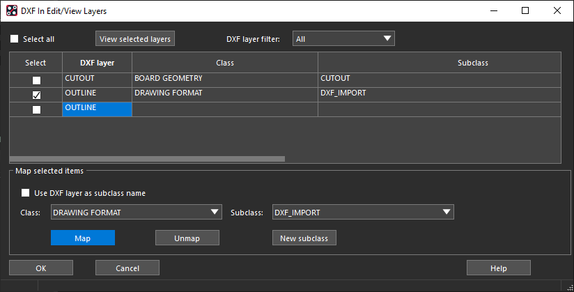
Step 19: Uncheck the Select option for Cutout. Repeat steps 16-18 to assign the Outline layer to the Drawing Format class and the created DXF_Import subclass.
Step 20: Click OK to save the mapping settings and close the window.
Step 21: Back in the DXF In window, select Import to load in the file.
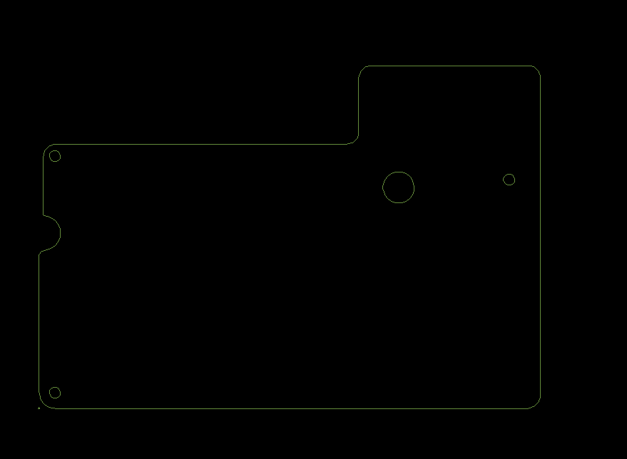
Step 22: The DXF geometry is loaded. Select Close in the DXF In window.
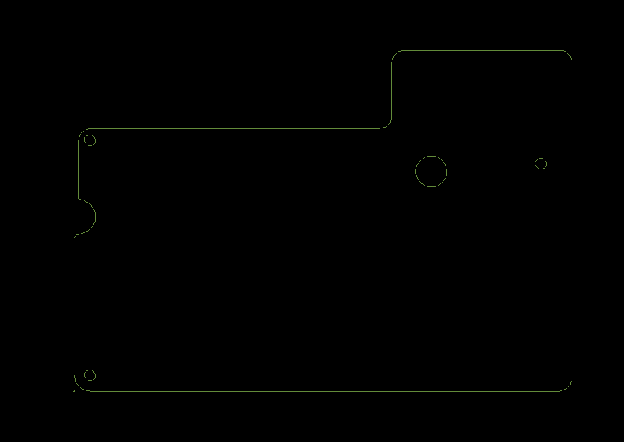
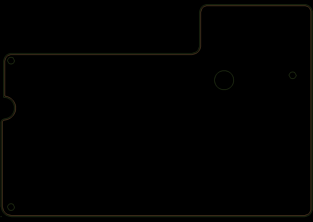
Step 23: Scroll up to zoom in and view the result in the PCB canvas. The design outline has been imported.
Changing Colors in the PCB
Note: Since new subclasses and the Design Outline subclass are shown in the same color by default, it is recommended to change one of them to avoid confusion.
Step 24: Select the Color button from the toolbar.
Step 25: Select the Drawing Format class.
Step 26: Select Cyan from the Available Colors table at the bottom of the window.
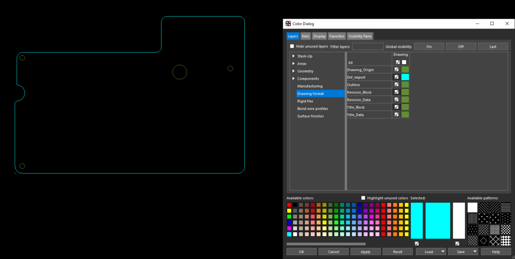
Step 27: Select the color block for DXF_Import to change the outline color.
Step 28: Click OK to save the settings and close the Color Dialog window.
Create a Board Outline from a DXF in OrCAD X
Step 29: Select Shape > Create Shape from Lines from the menu.
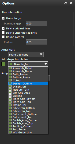
Step 30: In the Options panel, check the options for Delete Original Lines and Filled Shape.
Step 31: Select Board Geometry for the Active Class and Design_Outline for the Active Subclass.
Step 32: Click and drag to select all the lines and curves in the design outline. Right-click and select Done. This will change the outline class and subclass to Board Geometry and Design_Outline, respectively.
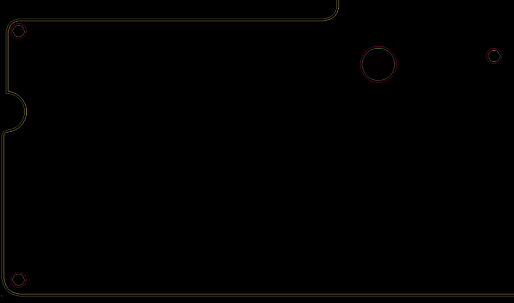
Creating Keepin Geometry
Note: DXF files may not include keepin or keepout geometry. This can be created in PCB Designer with the Z-copy feature. If the DXF file does include keepin or keepout geometry, these can be mapped to the corresponding layers in the design during the import.
Step 33: Select Shape > Z-Copy from the menu.
Step 34: The Z-Copy options are shown in the Options panel. Under Copy to Class/Subclass, select Package Keepin and All.
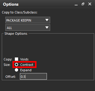
Step 35: For Size, select Contract and set the Offset to 0.5. This will replicate the design outline on the Package Keepin layer, contracting the outline to create a 0.5 mm spacing between the board edge and the package keepin.

Step 36: Click the board outline. The board geometry is copied and contracted on the Package Keepin layer.
Step 37: Select Route Keepin and All for the Z-Copy class and subclass.
Step 38: Click the board outline again. Route keepin geometry is added in a different color.
Creating Keepout Geometry
Step 39: To create keepout geometry for the board cutouts, select Package Keepout and All for the Z-Copy class and subclass.
Step 40: Select Expand under Size in the Options panel.
Step 41: Select the four cutouts on the board to create the keepout geometry.
Step 42: Select Route Keepout and All for the Z-Copy class and subclass.
Step 43: Set the Offset to 0 to copy the keepout geometry rather than the cutout geometry.
Note: The keepout geometry prevents the cutouts from being selected. Alternatively, package keepout geometry can be disabled in the Color Dialog window.
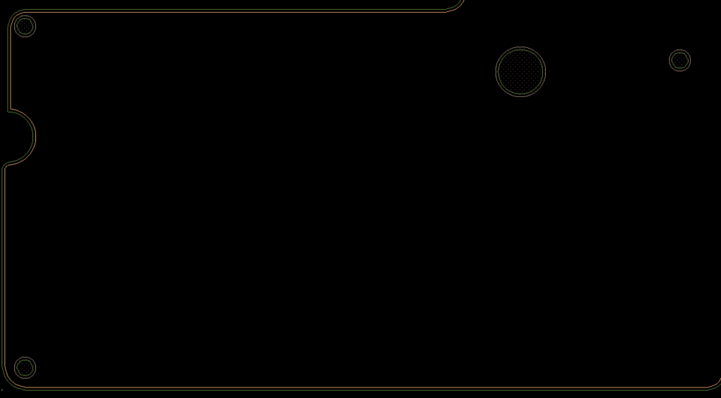
Step 44: Select the package keepouts. Route keepouts are created in a different color. Right-click and select Done.
Verifying the Board Geometry
Step 45: The board geometry can be verified in 3D. Select Display > 3D Canvas from the menu.
Step 46: The 3D Canvas Filter window opens. Leave the default settings and click OK.
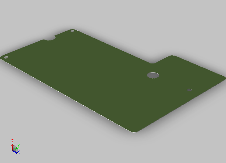
Step 47: View the board in the 3D canvas. The outline is shown as imported with the cutout holes in the correct places.
Note: Hold the middle mouse button and drag to pan the 3D canvas view. Hold Shift on the keyboard and drag the middle mouse button to rotate the view.
Wrap Up & Next Steps
Quickly create a board outline from a DXF file to accurately define the size, shape and features of the PCB with OrCAD X PCB Designer. Test this feature and more with a free trial of OrCAD. Get more how-tos for OrCAD at EMA Academy.
