Verifying adequate spacing is typically limited to traces on a single layer. However, in some applications spacing between traces on adjacent layers must be taken into consideration to meet safety and signal integrity requirements. With Z-DRC in Allegro Productivity Toolbox, easily perform Z-Axis clearance checks and analyze violations in OrCAD PCB Designer.
This quick how-to will provide step-by-step instructions on checking Z-axis clearance with Z-DRC in the Allegro Productivity Toolbox.
To follow along, download the provided files above the table of contents.
How-To Video
Configuring the Z-DRC Check
Step 1: Open the provided design in OrCAD PCB Designer Professional with the Allegro Productivity Toolbox option selected.
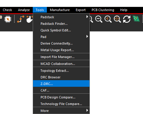
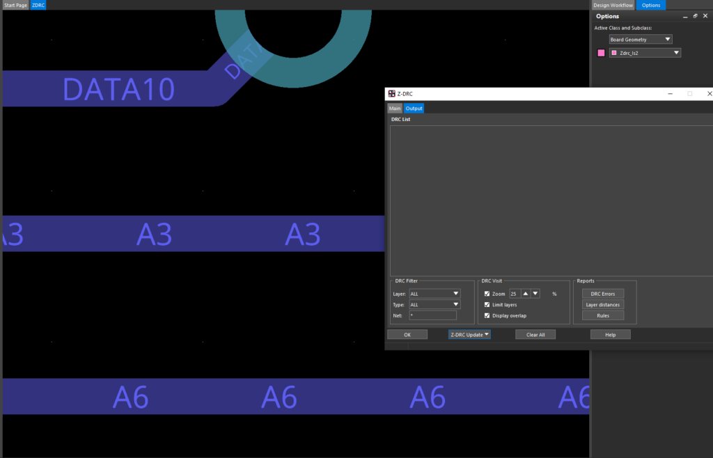
Step 2: Select Tools > Z-DRC from the menu. The Z-DRC window will open.
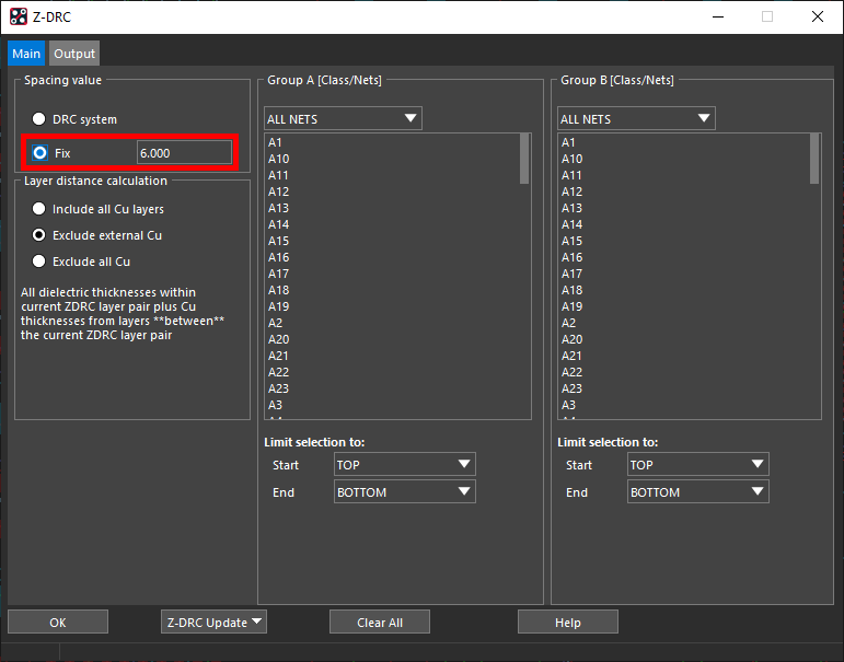
Step 3: Under Spacing Value, select Fix to set the spacing mode. The Fix value is set to 6 by default.
Note: Selecting Fix will give you the ability to define a spacing value manually. Choosing DRC system will calculate the actual value based on the spacing rules defined in the Constraint Manager.
Step 4: Under Layer Distance Calculation, select Exclude External Cu.
Note: Layer Distance Calculation allows users to account for thickness of copper layers.
- Include all Cu Layers: The thickness of all dielectric layers and all copper layers from the current layer span are summed.
- Exclude external Cu: The thickness of all dielectric layers and internal copper layers from the current layer span are summed.
- Exclude all Cu: Only the thickness of the dielectric layers from the current layer span are summed.
Step 5: From the Group A list, select net A3.
Note: When selecting nets, easily define the start and end layers for the Z-DRC check. Only objects (clines, shapes, pins and vias) included in the defined layer span will be considered.
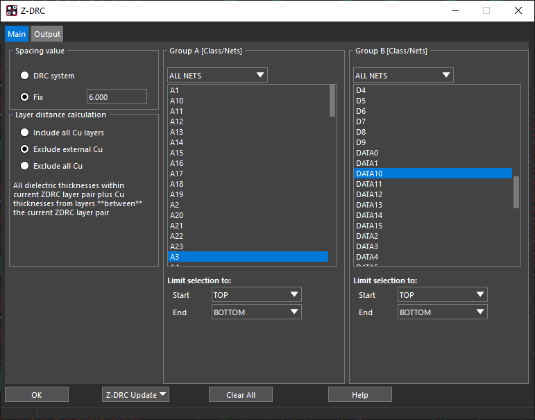
Step 6: From the Group B list, select net DATA10.
Note: This will check the nets from Group A against the nets from Group B. If no nets are selected from these lists, the Z-DRC check will not be run. Select multiple nets by holding CTRL on the keyboard.
Checking Z-Axis Clearance
Step 7: Select Z-DRC Update > Cleanup All DRC from the bottom of the window.
Note: Under the Z-DRC Update menu, two options are available:
- Retain Existing DRC: Keeps the DRC errors from previous Z-DRC checks.
- Clean up DRC: Removes any DRC errors that were previously generated but are no longer valid.
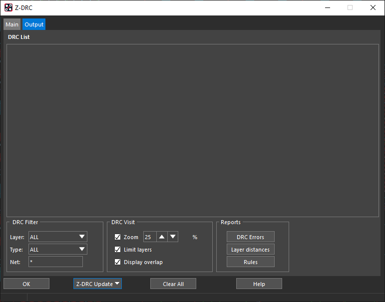
Step 8: Select the Output tab to view the results. The DRC check was run but no errors were found.
Modifying a Z-Axis Clearance Check
Step 9: Select the Main tab.
Step 10: Change the Fix value to 12.00.
Note: This will identify any traces on the selected nets that are less than 12 mils apart in the Z direction.
Step 11: Select Z-DRC Update > Cleanup All DRC from the bottom of the window.
Analyzing Z-DRC Errors and Reports
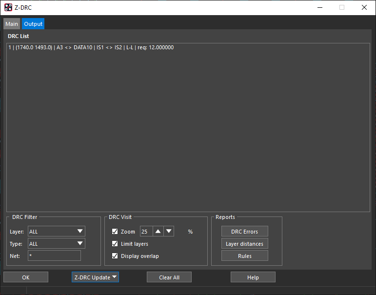
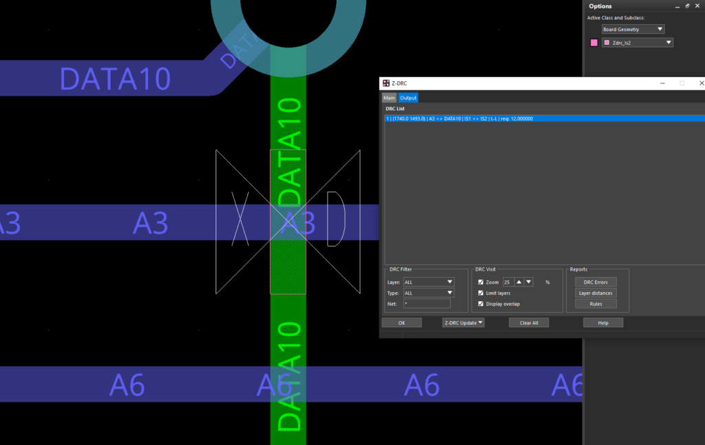
Step 12: Select the Output tab to view the generated error in the Z-DRC error and on the board.
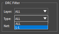
Note: If there are several DRC errors, results can be filtered by:
- Layer: Filters the violations to specific layer pairs between which a violation occurred.
- Type: The type of violation: For example, L-L: Layer-to-Layer.
- Net: The net on which the violation occurs.
Step 13: Under Reports, select DRC Errors.
Note: This saves the error report as zdrc_error_report.txt in the working directory and opens it in OrCAD.
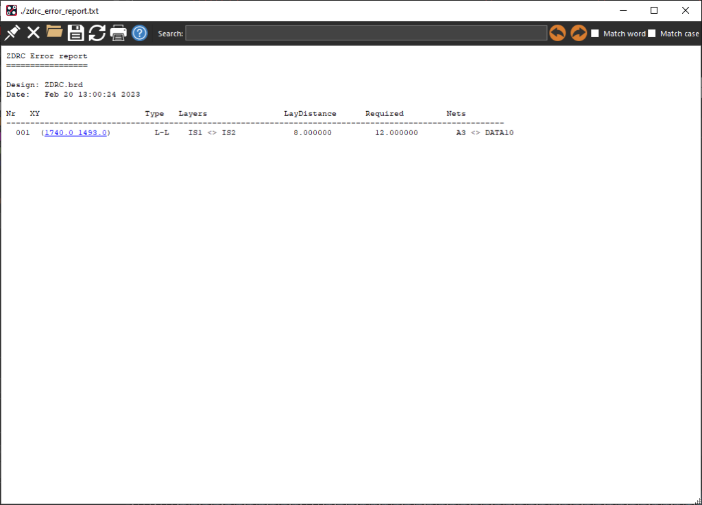
Step 14: View the DRC Report. Here we can see the distance is 8 mils and does not meet the defined requirement of 12 mils.
Note: The DRC Error report contains the following information:
- DRC error
- X and Y coordinates of the error
- Type or error
- Layers the error is between
- Actual Distance
- Required Distance
- Nets
Step 15: Under Reports, select Layer Distances.
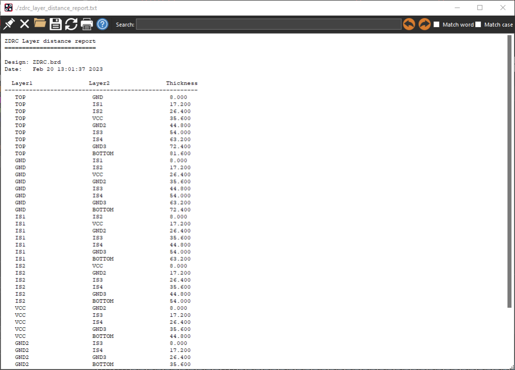
Note: This saves the layer distance report as zdrc_layer_distance_report.txt in the working directory and opens it in OrCAD. The Layer Distance report shows the calculated layer thicknesses for each layer combination.
Step 16: Select the error to view its location on the board.
Note: Visibility will adjust based on the selected parameters. The following options to view DRC errors can be configured:
- Zoom: Zoom to the location on the PCB
- Limit Layers: Only the layers involved in the violation will be displayed.
- Display Overlap: Since the algorithm used to calculate the Z-DRC is based on Boolean operations, select this option to view the amount of overlap graphically.
Step 17: Minimize the Z-DRC window.
Correcting Z-Axis Clearance Errors
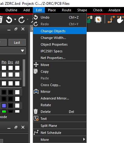
Step 18: Select Edit > Change Objects from the menu.
Step 19: Check the option for New Subclass.
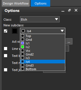
Step 20: Select layer IS4 from the New Subclass dropdown.
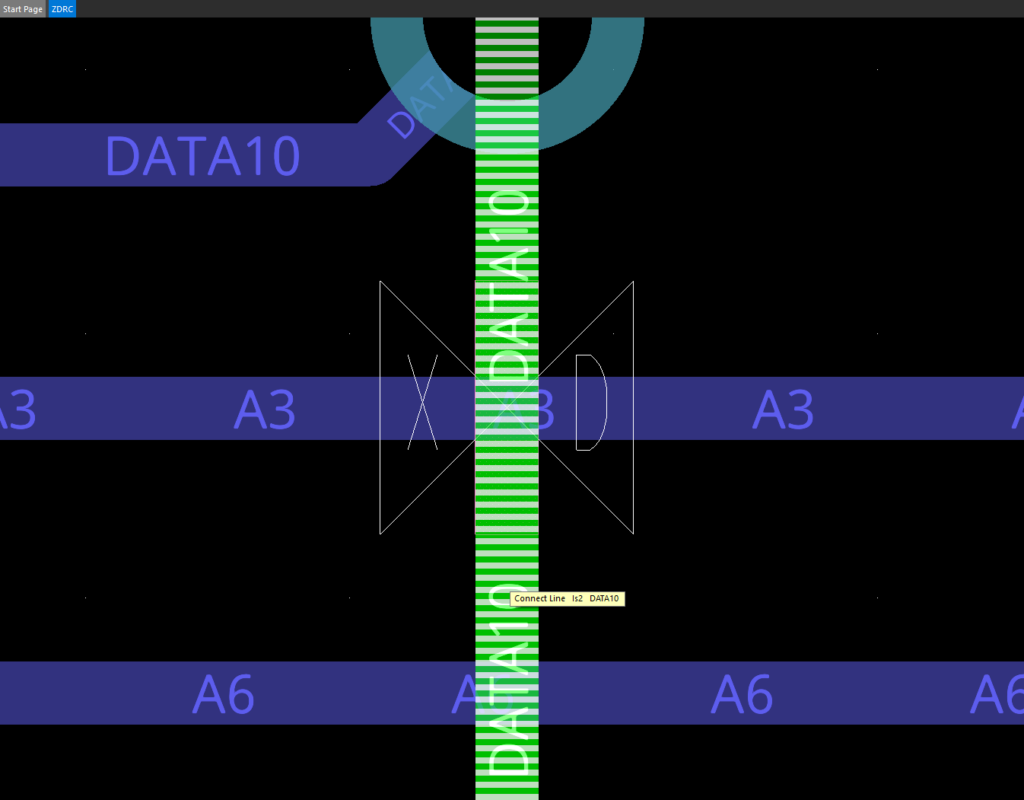
Step 21: Click the green DATA10 trace to change its layer to IS4. Right-click and select Done when finished.
Step 22: Back in the Z-DRC window, select Z-DRC Update > Cleanup All DRC from the bottom of the window.
Step 23: Select the Output tab. The error has been resolved and the marker has been cleared.
Wrap Up & Next Steps
Quickly check Z-Axis clearances and verify adequate spacing for traces between layers on the PCB with Z-DRC in the Allegro Productivity Toolbox. Learn more about the time-saving features included in Allegro Productivity Toolbox in this free webinar.

