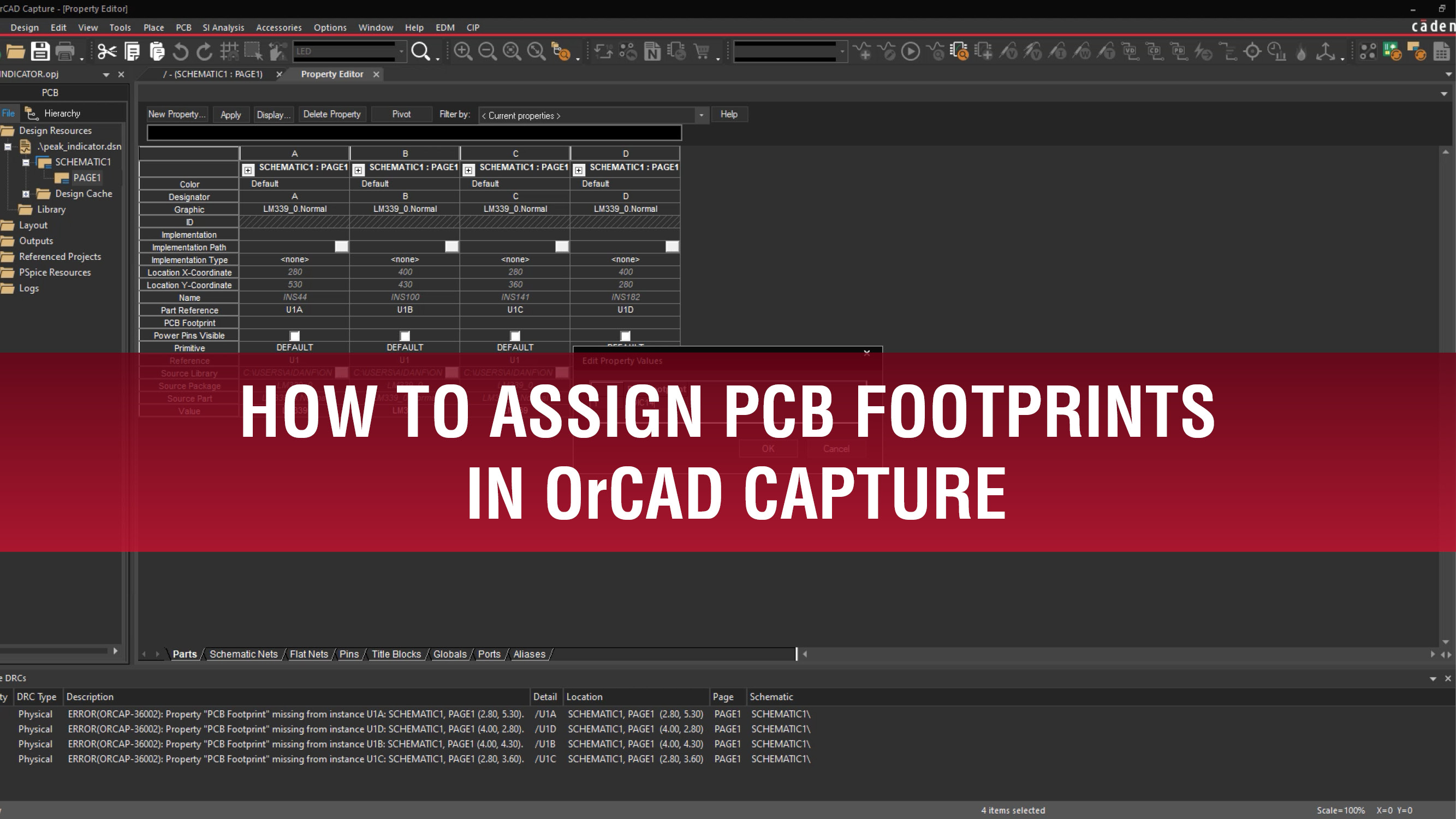
With your schematic completed and approved, the next step is to create the PCB. To accurately communicate the schematic design for PCB layout, a net list and parts list detailing the components and connections are necessary which requires you to assign PCB footprints to all components. OrCAD Capture makes it quick and easy to assign PCB footprints during the schematic design.
This quick how-to will provide step-by-step instructions on how to assign PCB footprints in OrCAD Capture.
To follow along, download the provided files above the table of contents.
How-To Video
 Open in New Window
Assign PCB Footprints in OrCAD
Step 1: Open the provided design in OrCAD Capture.
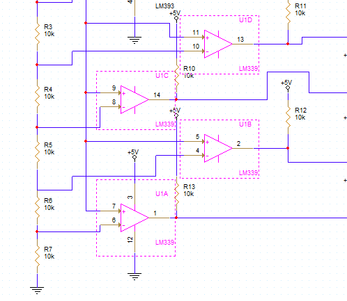
Step 2: Hold CTRL on the keyboard and select U1A-U1D.
Note: The CTRL key can be used to select multiple components at once, which is useful for batch processing.
Step 3: Right-click any of the selected components and select Edit Properties. The Property Editor tab opens.
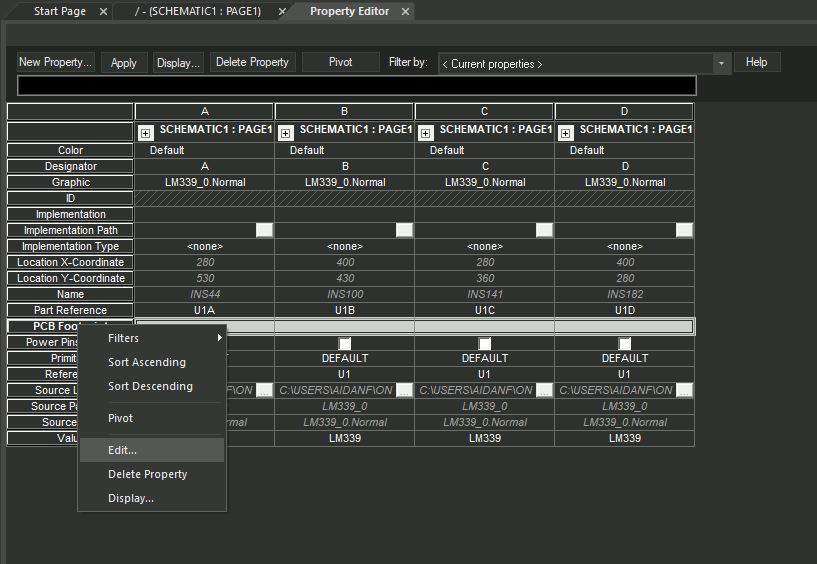
Step 4: Right-click the PCB Footprint category and select Edit.
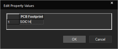
Step 5: The Edit Property Values window opens. Enter SOIC14 into the text field and click OK.
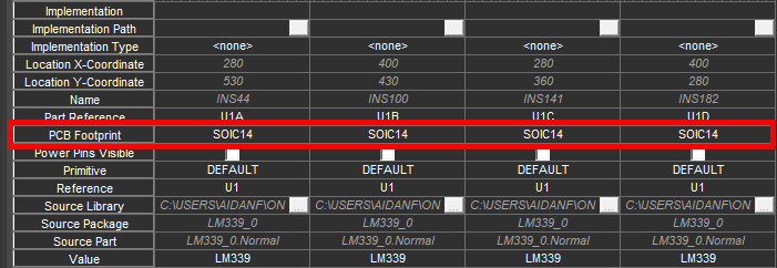
Step 6: This footprint is assigned to all components in the Property Editor tab. Click Apply and close the Property Editor tab.
Note: Repeat this process as needed for other components on the board.
Creating the PCB
With all component footprints assigned, they can be verified by creating the PCB layout.
Step 7: Select PCB > New Layout from the menu. The New Layout window opens.
Step 8: Leave the settings as the defaults and click OK to create the PCB layout.
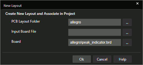
Note: The New Layout window can be used to define the layout folder and board names. If basing the layout on an existing board file, that board file can be specified in this window as well.
For more information on generating a PCB layout, view our how-to here.
Step 9: The Product Choices window opens for OrCAD PCB Designer. Select the appropriate license and click OK to open PCB Designer.
Verifying the PCB Footprint within the PCB
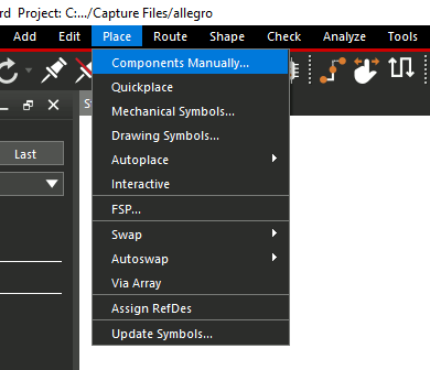
Step 10: In PCB Designer, select Place > Components Manually from the menu.
Step 11: The Placement window opens. Check U1 to place it in the canvas.
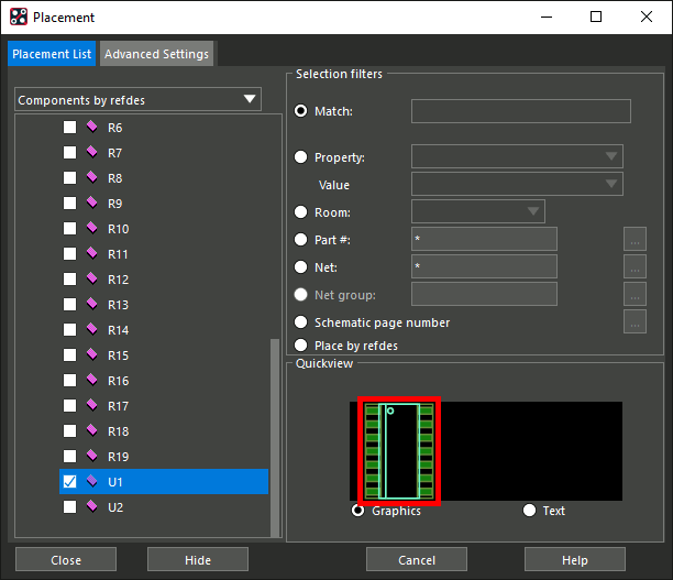
Note: A preview of the assigned footprint is shown to the right of the component list.
Step 12: Select Hide in the Placement window to make the PCB canvas easier to see.
Step 13: Click to place the component. The footprint for U1 is SOIC14, as assigned in Capture.
Wrap Up & Next Steps
Quickly assign PCB footprints in OrCAD and generate a usable PCB file from the schematic in OrCAD Capture. Test out this feature and more with a free trial of OrCAD. Want to learn more about Capture? Get access to free how-tos, courses, and walk-throughs at EMA Academy.

