With numerous IC devices in today’s PCB designs resulting in complicated power delivery networks, decoupling capacitors are often used as a source for instantaneous power; however, ineffective capacitors due to poor placement and high loop inductance can cause an unresponsive power delivery network and intermittent board failures. Easily evaluate the effectiveness of capacitor locations by extracting and analyzing the loop inductance with Sigrity Aurora. With the Power Inductance Workflow, you can:
- Simulate loop inductance between capacitors and ICs
- Simulate loop inductance for each power pin for IC devices
- Analyze tabular results
- Analyze visual overlays on the PCB
- Identify weak pins
- Ensure effective decoupling capacitors
- Generate a report for efficient communication
This quick how-to will provide step-by-step instructions on how to analyze loop inductance on your PCB to improve decoupling capacitor performance with the Power Inductance Workflow in Sigrity Aurora.
To follow along, download the provided files above the table of contents.
How-To Video

Activating the Power Inductance Workflow
Step 1: Open the provided design, LoopInductance.brd, in Sigrity Aurora 22.1.
Step 2: Select Analyze > Workflow Manager from the menu.
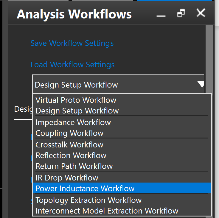
Step 3: Select the Power Inductance Workflow from the Analysis Workflow drop-down menu.
Note: This design is already configured for signal and power integrity analysis. To configure a new design for analysis, select Design Setup under General Setup. This will change the workflow to the Design Setup Workflow which outlines the required steps for accurate SI and PI analysis.
Configuring Analysis Options
Step 4: Under Analysis setup, choose Select Nets.
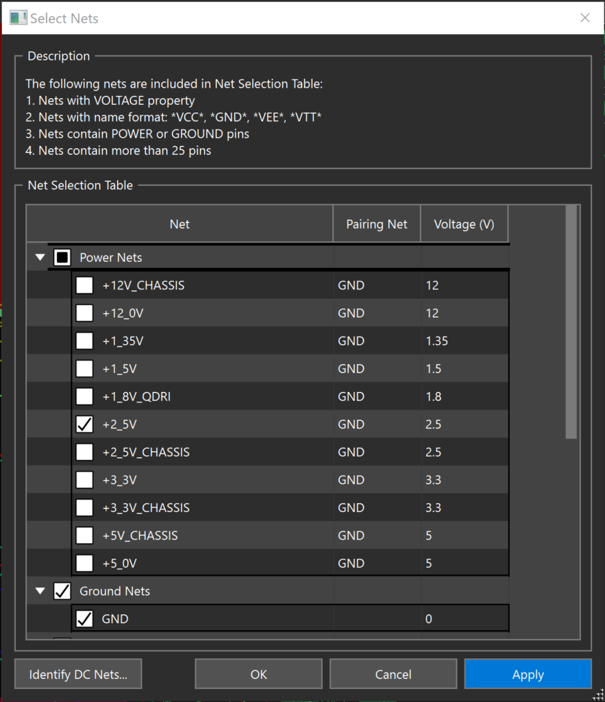
Step 5: Check the box for net +2_5V and click Apply.
Note: A green check will appear next to Select IC and decoupling Capacitors in the Power Inductance Workflow window. This indicates that the software has automatically identified the ICs and decoupling capacitors associated with the net selection.
Step 6: Click OK to close the net selection window.
Step 7: Choose Select ICs and Decoupling Capacitors.
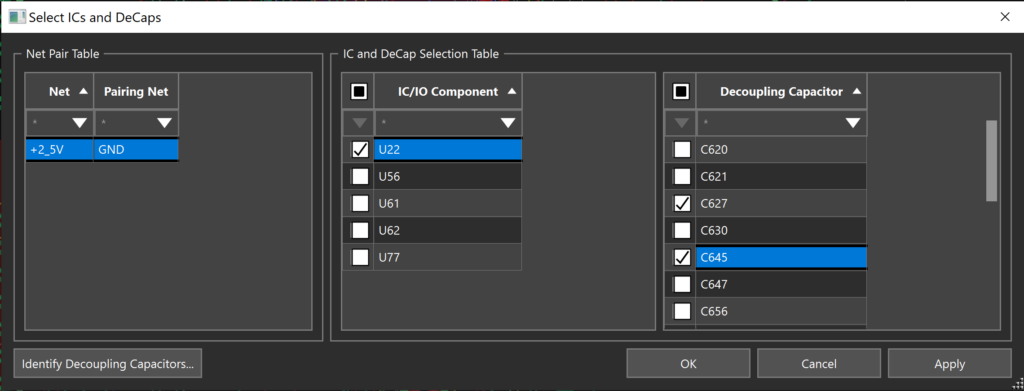
Step 8: Select the box next to IC/IO Component to deselect all the components then select U22.
Step 9: Select the box next to Decoupling Capacitor to deselect all the capacitors then select the following:
- C627
- C645
- C1009
Step 10: Select Apply and OK.
Step 11: Select Set up Frequency.
Step 12: Ensure the Solution Frequency is set to 1e+6 or 1MHz and click OK.
Note: Translator and Simulation options can also be configured in the IDA Power Inductance Analysis Parameters Setup Window.
Analyzing Loop Inductance
Step 13: Select Start Analysis.
Note: The progress of the simulation is shown in the Analysis section of the workflow. When the simulation is complete, a green check will appear and the results section will be activated.
Step 14: When the analysis is complete, ensure Capacitor to IC is selected under the View Modes drop-down menu.
Note: Results for IC Power Pin can also be analyzed with selection under View Modes.
Step 15: Select View DeCap Loop Inductance Tables.
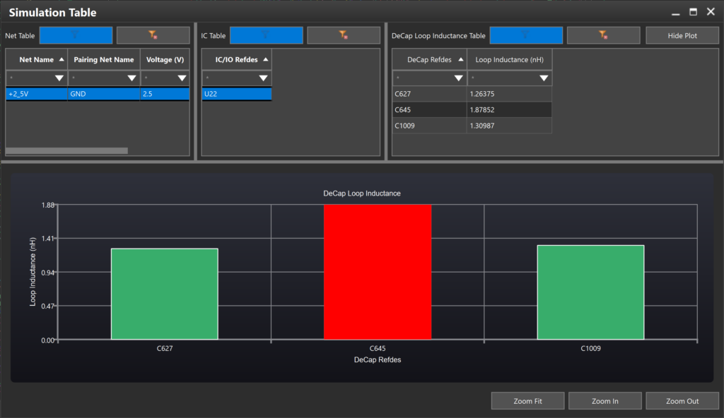
Step 16: Review the tabular and graphical results of the Capacitor to IC loop inductance. Capacitor C645 has the highest loop inductance with a value of 1.878.
Note: Adjust the tabular and graphical result panes as needed. While there is no set value to indicate a poor loop inductance, the ideal value for the capacitor to IC loop inductance is 1.
Step 17: Close the DeCap Loop Inductance Table.
Step 18: Back in the Power Inductance Workflow, select View DeCap Loop Inductance Visions.
Step 19: View the loop inductance overlay on the PCB.
Note: Here you can view a color-coded overlay on the PCB for easy identification of decoupling capacitors that can be improved. Move the color meter on the right side of the screen to only show capacitors with high loop inductance values.
Step 20: Select View DeCap Loop Inductance Visions again to close the overlay.
Generating a Report
Step 21: Under Analysis Results in the Power Inductance Workflow, select Create Report.
Note: The report automatically includes tabular and graphical results for Capacitor to IC Loop Inductance and IC Power Pin.
Step 22: Select Save. Browse to the desired location, provide a name for the file, and click Save.
Note: Generating and saving the report of the loop inductance results will improve communication between stakeholders.
Step 23: Close the report and tabular results.
Improving Decoupling Capacitor Placement
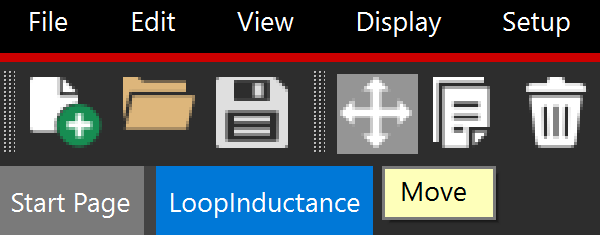
Step 24: Select the Move button on the toolbar.
Step 25: Right-click on the canvas and select Options > Slide Etch (prototype).
Step 26: In the Find Panel, check the box next to Pins to turn off the selection.
Note: This will make it easier to select the capacitor. If the Find window is not visible, select View > Windows > Find from the menu. Zoom into the area with C645 as needed.
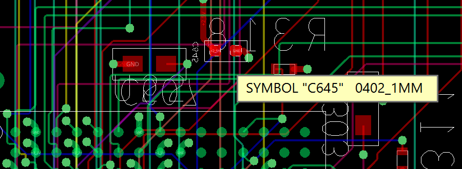
Step 27: Select decoupling capacitor C645.
Step 28: Move C645 closer to the IC and click to place.
Step 29: Click a via for the capacitor fanout and move it closer to the capacitor. Click to place.
Step 30: Select the other via in the capacitor fanout and move it closer to the capacitor. Click to place.
Step 31. Select Route > Slide from the menu.
Step 32: Select a trace with a design rule error. Move the trace and click to place.
Note: Repeat this process as needed until all design rule errors are resolved.
Step 33: Right-click and select Done.
Analyzing the Improved Loop Inductance
Step 34: In the Analysis Workflow window, select Start Analysis.
Step 35: When prompted to save existing results, select Ignore to run the simulation again without saving the previous results.
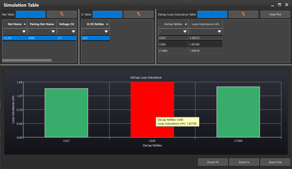
Step 36: When the analysis is complete, select View DeCap Loop Inductance Tables. The loop inductance of C645 has improved from 1.878 to 1.43.
Note: Results will vary based on component placement.
Wrap Up & Next Steps
Create a responsive power delivery network by analyzing loop inductance and the effectiveness of decoupling capacitors in your PCB design with the Power Inductance Workflow in Sigrity Aurora. Get our free e-book to learn more about meeting high-frequency power demands with decoupling capacitors.
