High-voltage applications can require additional planning and careful design to ensure the safety and reliability of your end product and adhere to industry standards. Having high-voltage traces too close together can lead to potential issues such as:
- Arcing
- Signal Interference
- Stray E-Fields
- Parasitic Capacitance
Often slots are required between high-voltage objects when there is not sufficient room on the PCB but analyzing the creepage distance becomes more difficult. New in Allegro X 23.1 is the ability to configure checks for creepage and clearance, automatically calculate the creepage and clearance distances, and view color-coded analysis results directly on the PCB canvas.
This quick how-to will provide step-by-step instructions on how to set and use creepage and clearance constraints in Allegro X Venture.
How-To Video

Creating a High Voltage Constraint Set
Step 1: Open a design in Allegro X Venture.
Step 2: Select Setup > Constraints > Constraint Manager from the menu.
Step 3: Select the Electrical domain from the Worksheet Selector.
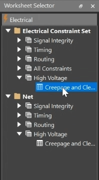
Step 4: Select the Electrical Constraint Set > High Voltage > Creepage and Clearance worksheet.
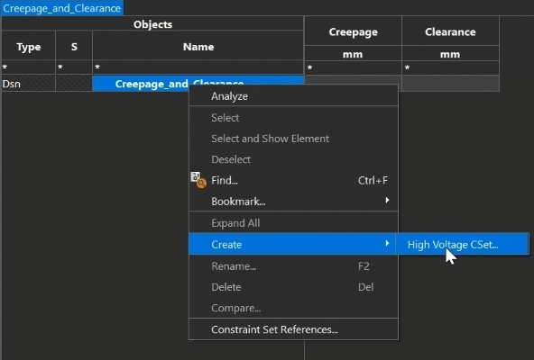
Step 5: Right-click the Creepage_and_Clearance cell and select Create > High Voltage CSet.
Step 6: Name the Cset 48V_ISO and click OK.
Step 7: Enter 2.54 into the cell under the Creepage column for the new Cset for a creepage of 2.54mm.
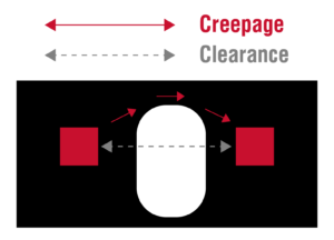
Note: Creepage defines the distance between high-voltage nets between multiple layers or around a non-plated hole. Clearance defines the direct distance between high-voltage nets on the same layer.
Step 8: Right-click the Cset and select Create > High Voltage CSet.
Step 9: Name the Cset 48V_Intra.
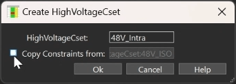
Step 10: Uncheck Copy Constraints From to create a blank constraint set. Click OK.
Step 11: Enter 0.720 into the cell under the Creepage column for the 48V_INTRA Cset for a creepage of 0.720mm.
Assigning a High Voltage Constraint Set
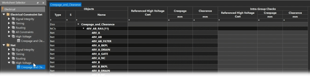
Step 12: Select the Net > High Voltage > Creepage and Clearance worksheet.
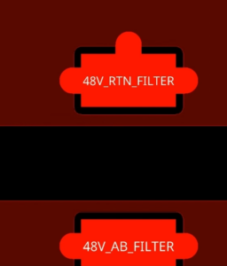
Step 13: Under the Referenced High Voltage CSet column for 48V_AB_RAIL and 48V_RTN_RAIL, select 48V_ISO from the dropdown.
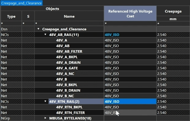
Note: The 48V_ISO CSet is automatically assigned to all nets in the group.
Step 14: Under Intra-Group Checks, select the 48V_INTRA Cset in the Referenced High Voltage CSet column for 48V_AB_RAIL and 48V_RTN_RAIL.
Note: Creepage and clearance to nets within the same class will be checked against the intra-group Cset, while creepage and clearance to nets outside will be checked with the regular high voltage Cset.
Step 15: Close the Constraint Manager.
Checking for Creepage and Clearance Violations
Step 16: Select the Update DRC button from the toolbar.
Step 17: Select View > Vision Manager from the menu. The Visions panel opens.
Step 18: Select Creepage/Clearance Vision from the Vision Manager dropdown.
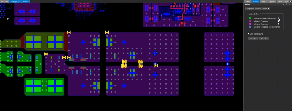
Step 19: Under Vision Colors, check the option for Meets Creepage/Clearance to highlight constrained nets that meet the creepage and clearance requirements.
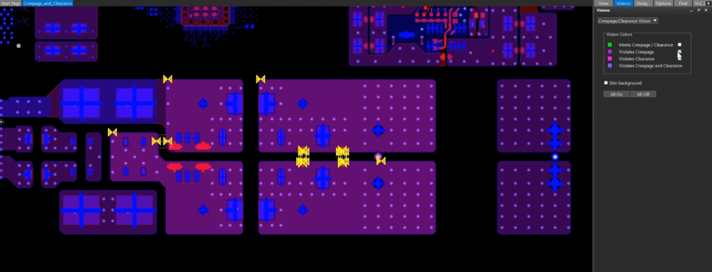
Step 20: Uncheck Meets Creepage/Clearance and check the option for Violates Creepage to view the nets that violate the creepage values.
Step 21: Uncheck Violates Creepage.
Resolving Creepage and Clearance Violations
Note: Several methods exist to correct high voltage violations, depending on the problem.
Step 22: In the Visibility panel, turn off visibility for the Top layer so only the Bottom layer (with the violations) is visible.
Step 23: Select Setup > Application Mode > Placement Edit from the menu.
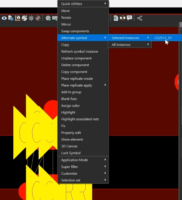
Step 24: Right-click a component with violations and select Alternate Symbol > Selected Instances > CS2512_01.
Step 25: You will be prompted to rip up the etch. Click Yes to proceed.
Step 26: View the results. The component is replaced and the DRCs are removed.
Expanding Clearances
Step 27: In the Visibility panel, turn on visibility for the Top layer. More violating components appear, including a pin between two high voltage planes.
Step 28: Select Setup > Application Mode > General Edit from the menu.
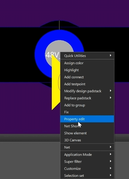
Step 29: Right-click the pin and select Property Edit.
Step 30: Select Dyn_Clearance_Oversize_Array from the Available Properties list.
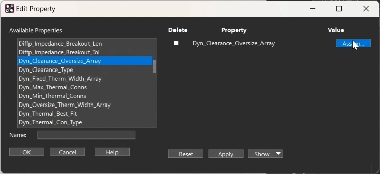
Step 31: Select Assign under Value.
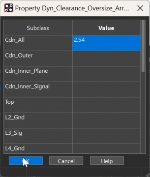
Step 32: Enter 2.54 for the Cdn_All subclass value. Click OK.
Step 33: Click Apply and OK in the Edit Property window.
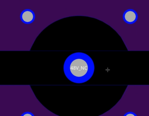
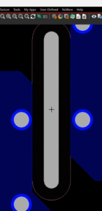
Step 34: View the results. The spacing between the pin and planes has widened and the DRCs are removed.
Adding a Slot
Note: If creepage rules are violated by vias, a non-plated hole must be added between them. This can be done by adding a slot hole or drawing a cutout.
Step 35: Select Place > Manually from the menu.
Step 36: Select Mechanical Symbols from the dropdown.
Step 37: Select and check NPTH_SLOT_31X325 to place the non-plated slot.
Step 38: Click to place the symbol between the two vias. The DRC violation is cleared.
Note: The violation can also be cleared by drawing a cutout.
Step 39: Right-click and select Oops to cancel the placement.
Step 40: Click Close in the Placement window.
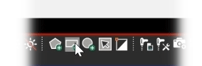
Step 41: Select Add Rectangle from the toolbar.
Step 42: In the Options panel, select Board Geometry and Cutout as the active class and subclass.
Step 43: Under Shape Creation, select Place Rectangle. Enter 0.8 for the width and 8.2 for the height.
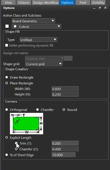
Step 44: Select Round under Corners. Select Trim and enter 0.4.
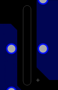
Step 45: Click to place the rectangle. Right-click and select Done. The DRCs are removed.
Wrap Up & Next Steps
Quickly create and check creepage and clearance constraints in Allegro X to guarantee the safety and reliability of your high-voltage PCB designs. Upgrade to 23.1 to test out this and other new features in Allegro.

