Every PCB manufacturer has a different set of minimum requirements for manufacturability. If boards do not meet these requirements manufacturing can be halted or the board can be produced incorrectly, resulting in increased design time and cost for the project. With OrCAD, designers can adhere to manufacturing requirements during PCB layout and design for manufacturing, a crucial aspect to first-pass board success.
This quick how-to will provide step-by-step instructions on how to implement manufacturing requirements as constraints to guarantee manufacturability with the constraint manager in OrCAD PCB Designer.
To follow along, download the provided design above the table of contents.
How-To Video
 Open in New Window
Determine Manufacturer Requirements
Step 1: Open a web browser and navigate the desired manufacturer’s website. In this example, we will use Sierra Circuits.
Step 2: Select PCB Products > Web PCB from the menu.
Note: Many manufacturers will have similar pages on their websites where detailed information can be found about their manufacturing capabilities and requirements.
Step 3: Scroll down to view the manufacturing and assembly capabilities table. Here you can review Sierra Circuits’s capabilities and requirements for Standard PCBs. For detailed information such as Advanced or Micro Board capabilities, select PCB Products > Rigid PCBs from the menu. Advanced and Micro capabilities typically have an associated cost due to the advanced equipment required to manufacture the board and tighter tolerances.
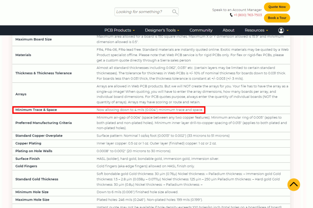
Step 4: Scroll down to the information and capabilities table. Locate the capabilities for trace width and spacing:
- Min Trace and Space: 0.004” = 4 mil
Note: Fabricating a board at the bare minimum values may cost more and have a longer turnaround time. Consult with your manufacturer regarding additional costs.
Some manufacturers have partnered with Cadence, detailing their requirements in the DFM Partner Portal for simplified rule assignment.
Define Manufacturer Constraints
Step 5: Open the provided design in OrCAD PCB Designer.
Step 6: Select Setup > Constraints from the menu or the Constraints button from the toolbar.
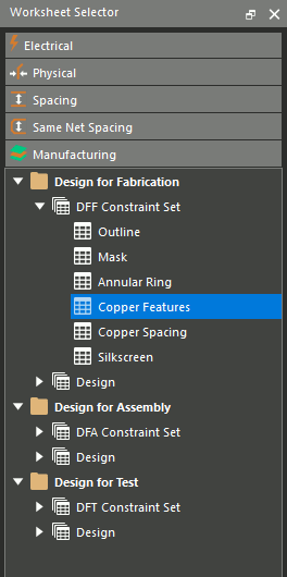
Step 7: Select the Manufacturing domain from the worksheet selector. Expand the Design for Fabrication and the DFF Constraint Set sections. Select the Copper Features worksheet.

Step 8: In the Name column, click the <Create New> placeholder. Name the Cset Sierra Circuits and click OK.
Note: Constraint sets can be created for various manufacturers and loaded into the software to easily adhere to manufacturing requirements and capabilities for differing manufacturers.
Step 9: To adhere to manufacturing requirements for traces, select the Minimum Line Width cell and enter 4 mils.
Step 10: Select the Copper Spacing worksheet in the DFF Constraint Section.
Step 11: Under the New Cset column, select the blank cell. Name the constraint set Sierra Circuits and click OK.
Step 12: Expand Trace to and select the cell for Trace. Define a value of 4 mils.

Step 13: Back on the Sierra Circuits webpage, review the Preferred Manufacturing Capabilities. Here we can determine copper spacing requirements.
Step 14: Back in the constraint manager in OrCAD PCB, expand Shape To.

Step 15: To adhere to manufacturing requirements for copper spacing, add the following constraints:
- Shape to Shape spacing = 4 mils
- Shape to Trace spacing = 4 mils
- All Pin Pads = 4 mils
- All Via Pads = 4 mils
Note: These constraints can be derived from Minimum air-gap of 0.004”.
Step 16: Under the Name column, select <Create New>. Name the constraint set Sierra Circuits_Inner and click OK.
Step 17: To adhere to manufacturing requirements for copper spacing on internal layers, expand Hole under Trace and Shape and add the following constraints:
- Trace to Non-Plated Hole = 13 mils
- Trace to Trace Hole = 13 mils
- Trace to Shape Hole = 13 mils
- Shape to Non-Plated Hole = 13 mils
- Shape to Trace Hole = 13 mils
- Shape to Shape Hole = 13 mils
Note: These constraints can be derived from Minimum inner-layer drill-to-copper spacing of 0.013”.

Step 18: Back on the Sierra Circuits webpage, review the Preferred Manufacturing Capabilities again. From the minimum annular ring of 0.005” we can determine the annular ring requirements.
Step 19: Back in the constraint manager in OrCAD PCB, navigate to the Annular Ring worksheet.
Step 20: Under the Name column, select <Create New>. Name the constraint set Sierra Circuits and click OK.

Step 21: To adhere to manufacturing requirements for annular rings, add the following constraints:
- All Pins Hole to Pad = 6 mils
- All Vias Hole to Pad = 6 mils

Step 22: Back on the Sierra Circuits webpage, review the Silkscreen/Legend again. From this we can determine the minimum line width for silkscreen and legends.
Step 23: Back in the constraint manager in OrCAD PCB, navigate to the Silkscreen worksheet.
Step 24: Under the Name column, select <Create New>. Name the constraint set Sierra Circuits and click OK.

Step 25: To adhere to manufacturing requirements for silkscreen, add the following constraints:
- Min Width (line, arc, shape) = 6 mil
- Min Length (line, arc) = 6 mil
- Text Overlap = Off
- Text Under Component = On
Assign Manufacturing Constraints
Step 26: In the Manufacturing domain, expand the Design for Fabrication > Design section. Select the Annular Ring worksheet.
Step 27: Expand the Primary row.

Step 28: Click the Referenced DFF CSet cell for Conductor and select SIERRA CIRCUITS. The constraints are automatically assigned to the conductor layers.
Step 29: Select the Design > Copper Features worksheet.
Step 30: Expand the Primary row.
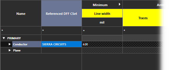
Step 31: Click the Referenced DFF CSet cell for Conductor and select SIERRA CIRCUITS. The constraints are automatically assigned to the conductor layers.
Step 32: Select the Design > Copper Spacing worksheet.
Step 33: Expand the Primary and Conductor rows.

Step 34: Click the Referenced DFF CSet cell for Top and select SIERRA CIRCUITS.
Step 35: Click the Referenced DFF CSet cell for Bottom and select SIERRA CIRCUITS.
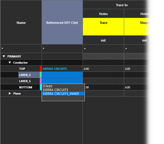
Step 36: Click and drag to select the Referenced DFF CSet cells for LAYER_2 and LAYER_5. Select SIERRA CIRCUITS_INNER from the dropdown.
Note: Inner layers often have tighter requirements than outer layers.
Step 37: Click the Referenced DFF CSet cell for Plane and select SIERRA CIRCUITS_INNER.
Step 38: Select the Design > Silkscreen worksheet.
Step 39: Expand Primary and Mask.

Step 40: Click and drag to select the Referenced DFF CSet cells for Soldermask_Top, Pastemask_Top, Pastemask_Bottom, and Soldermask_Bottom. Select SIERRA CIRCUITS.
Turn On DFM Design Rule Checks
Note: Before any constraint checks are performed, the DFM check modes must be activated.
Step 41: Select Analyze > Analysis Mode from the Constraint Manager menu. The Analysis Modes window opens.
Step 42: Select Design for Fabrication > Outline from the sidebar.
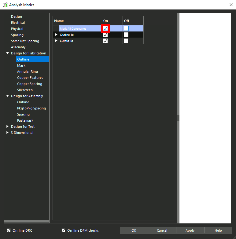
Step 43: A table of checks appears. Select On under Mark All Constraints to activate all constraint checks.
Step 44: Select Design for Fabrication > Mask and select On under Mark All Constraints.
Step 45: Select Design for Fabrication > Annular Ring and select On under Mark All Constraints.
Step 46: Select Design for Fabrication > Copper Features and select On under Mark All Constraints.
Step 47: Select Design for Fabrication > Copper Spacing and select On under Mark All Constraints.
Step 48: Select Design for Fabrication > Silkscreen and select On under Mark All Constraints.
Step 49: Click OK to save the settings and close the window.
Step 50: Close the Constraint Manager. The constraint sets have been assigned and checks have been activated.
Adhere to Manufacturing Requirements
Note: A Design Rule Check can be performed to identify potential errors and adhere to manufacturing requirements during the PCB layout to reduce manufacturing delays and design respins.
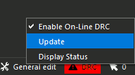
Step 51: With the constraints updated, the Design Rule Check (DRC) cache is out of date. Select the DRC button in the bottom-right corner of the screen and select Update.
Note: This button is red when the cache is out of date, yellow when errors exist, and green when no errors are present.
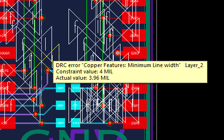
Step 52: A cluster of DRC markers have appeared throughout the board. Zoom in and hover your cursor over one of the errors for additional information.
Step 53: As an example, we will correct the errors on the right side of the board by changing trace widths. Zoom in on the bottom-right corner.
Step 54: Select Edit > Change Objects from the menu.
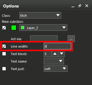
Step 55: Check the option for Line Width and enter 8.
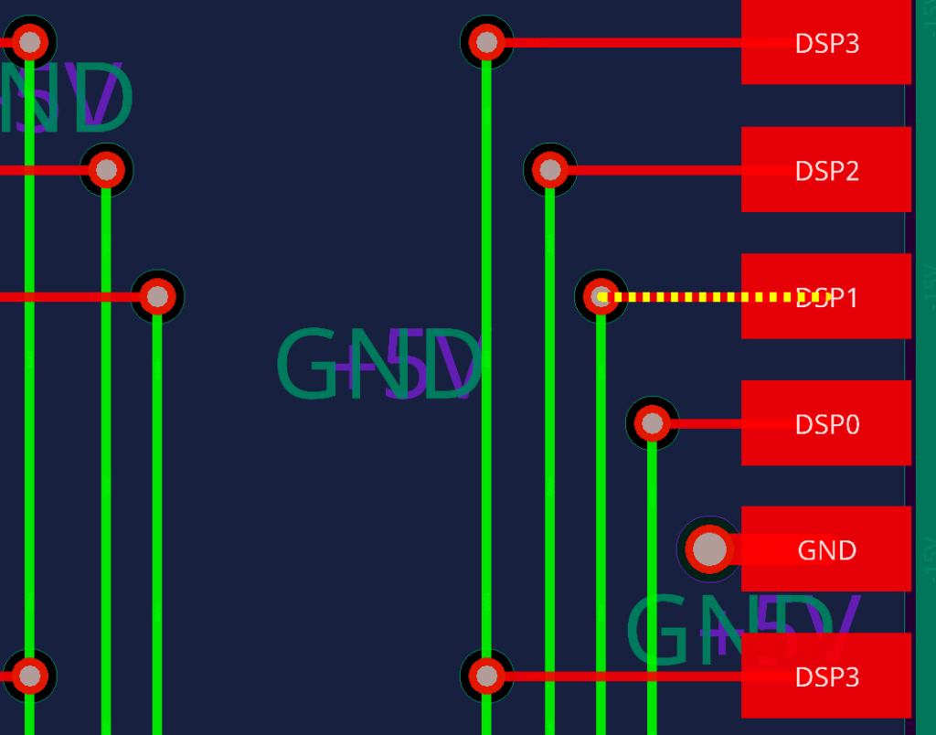
Step 56: Click the traces with markers labeled “fl” on the board to thicken the lines and remove the errors. When finished, right-click and select Done.
Note: Select the Nets option in the Find panel to thicken the entire net at once rather than individual traces.
Step 57: Select the DRC button and Update. There are still DRCs in the design, so the button remains yellow, but the count has decreased.
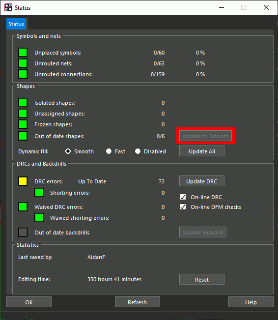
Note: If the button remains red, select the button and Display Status. Click Update to Smooth under Shapes and click OK. Select the button and Update again.
Export Manufacturing Constraints
Step 58: Select Setup > Constraints from the menu or the Constraints button from the toolbar.
Step 59: Select File > Export > Constraints.
Step 60: Under Contents, uncheck the following:
- User Property Definitions
- Electrical Constraints
- Physical and Spacing Constraints
- Properties
This will leave only Manufacturing Constraints selected.
Step 61: Name the file Sierra_Circuits.dcfx and click Save.
Note: To import the set, select File > Import > Constraints. Select Sierra_Circuits.dcfx and click Open. A difference report will be shown.
The constraints added in this tutorial are not exhaustive and only provide an example of the capabilities included in OrCAD to manage manufacturing requirements and capabilities.
Wrap Up & Next Steps
Adhere to manufacturing requirements and design a manufacturable board the first time to avoid derailing your project with rejections and stalled fabrication with the constraint manager in OrCAD PCB Designer. Test out this feature and more with a free trial of OrCAD.