When working with high-speed signals, having a good return path is crucial for signal integrity. For some high-speed nets, return path vias should be incorporated every time a via is placed. While these can be added manually after routing is complete, it can be tedious and increase the possibility of errors. With the high-speed option in Allegro PCB Designer, return path vias can be configured and added automatically during routing.
This quick how-to will provide step-by-step instructions on how to configure and add return path vias when routing single nets with the high-speed functionality in Allegro PCB Designer.
How-To Video
Configuring Return Path Via Settings
Step 1: Open the desired design in Allegro PCB Designer with the High-Speed Option enabled.
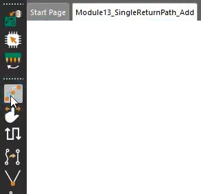
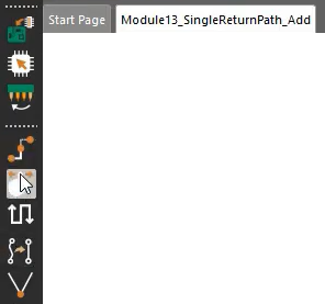
Step 2: Select Route > Connect from the menu or the Add Connect icon from the toolbar.
Step 3: Click to start routing a trace.
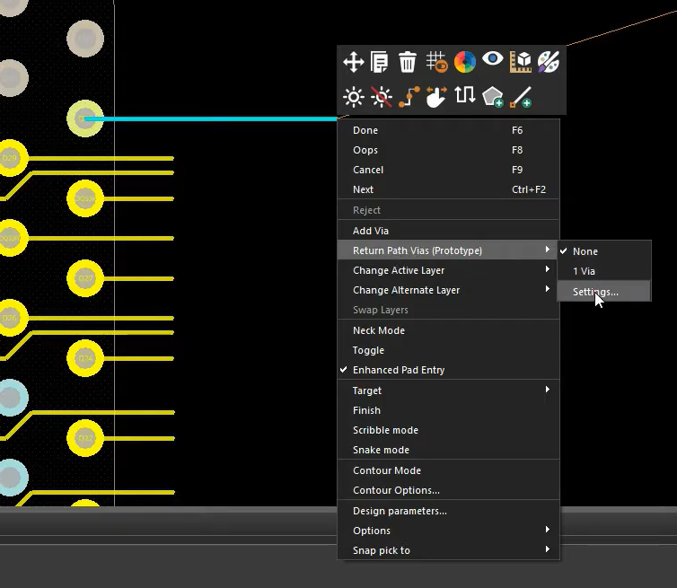
Step 4: To configure settings, right-click and select Return Path Vias > Settings.
Note: A warning may appear that the feature is in the prototype phase. Click OK.
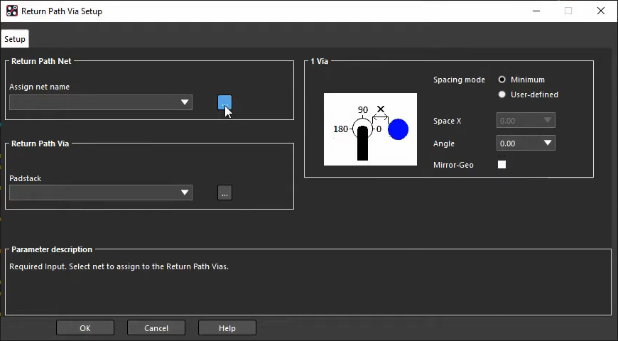
Step 5: The Return Path Via Setup window opens. Select the ellipsis for Return Path Net to assign a net name.
Step 6: Select the desired net name and click OK.
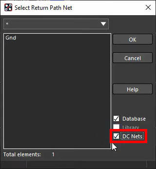
Note: If a voltage property has been defined for nets in the design, select DC Nets to filter the nets.
Step 7: Select the ellipses for Return Path Via to select the padstack.
Step 8: Select the desired padstack and click OK.
Note: You can filter padstacks from:
- The database
- The library
- What is allowed by the net’s physical constraint set
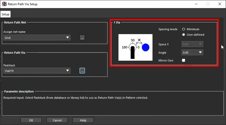
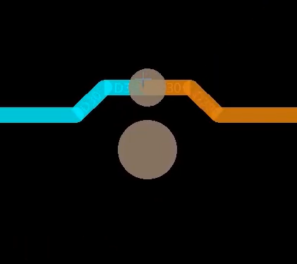
Step 9: Set the desired via spacing under 1 Via. By default, the minimum spacing is configured.
Note: The 1 via pattern adds one return path via next to one of the trace vias. Here you can configure the:
- Space X: Circumference-to-circumference distance of the vias.
- Angle: The angle at which the return path via is located with respect to the trace via.
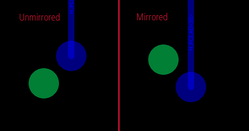
- Mirror-Geo: Mirrors the location of the return path via as shown below.
Step 10: Click OK.
Placing Return Path Vias
Step 11: Right-click in the canvas and select Return Path Vias > 1 Via to associate the via.
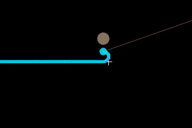
Step 12: Double-click while routing to activate via placement. Via placement mode will activate as normal and the return path via will attach to your cursor separate from the trace.
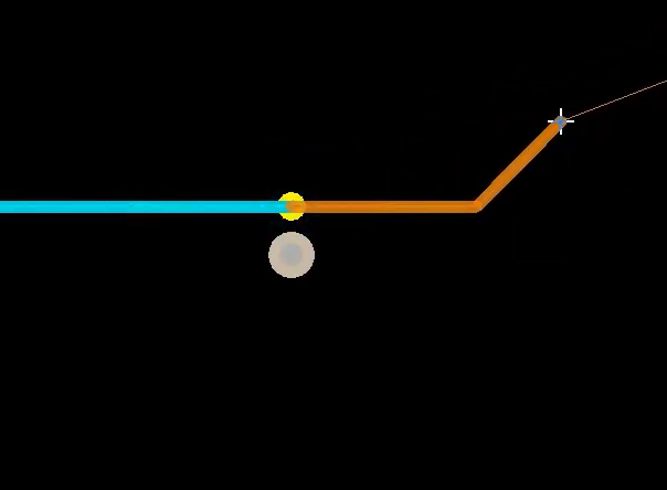
Step 13: Click to place the vias.
Step 14: Continue routing the trace. Right-click and select Done when finished.
Adjusting Vias
Step 15: Select Route > Slide from the menu or the Slide button from the toolbar.
Step 16: Select one of the vias. The trace and return path via are both attached to the cursor.
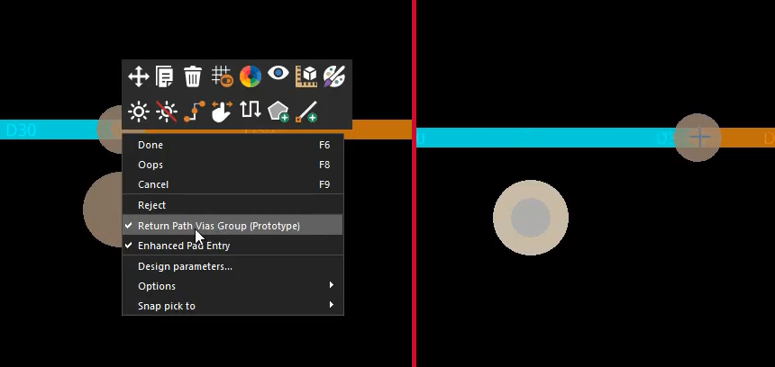
Step 17: To adjust each via separately, right-click and de-select Return Path Vias Group while the group is selected.
Note: If you reactivate this option after moving one of the vias, the trace and return path vias will lock together as they are.
Step 18: When finished, right-click and select Done.
Wrap Up & Next Steps
Accelerate the PCB layout for high-speed designs and quickly add return path vias while routing with the high-speed functionality in Allegro PCB Designer. Learn more about solving common issues for high-speed designs with our e-book.

