After fabricating multilayer board designs, testing is performed to guarantee functionality and performance of the PCB. If an error is found, instead of scrapping the boards, modifications can be made to salvage the fabricated PCBs. When designers add resistive mask layers, such as conductive ink, modifications can be made to the design and printed by the fabrication house, saving thousands of dollars and keeping your project on-time. OrCAD PCB Designer allows you to easily define and add resistive mask layers in your PCB designs to efficiently make the required design modifications.
This quick how-to will provide step-by-step instructions on how to create resistive mask layers with the cross-section editor in OrCAD PCB Designer.
To follow along, download the materials provided above the table of contents.
How-To Video
 Open in New Window
Add Resistive Mask Layers
Step 1: Open the desired design in OrCAD PCB Designer.
Step 2: Select Setup > Cross-Section from the menu or the Cross-Section button from the toolbar.
Step 3: Right-click the top conductor layer and select Add Layers.
Step 4: The Add Layers window opens. Specify the new layer position as Above Conductor TOP.
Step 5: For the Layer Type, expand and select Mask > Design-defined Mask Layers > Top > Carbon Top.
Step 6: Under Layer Function, select Resistive.
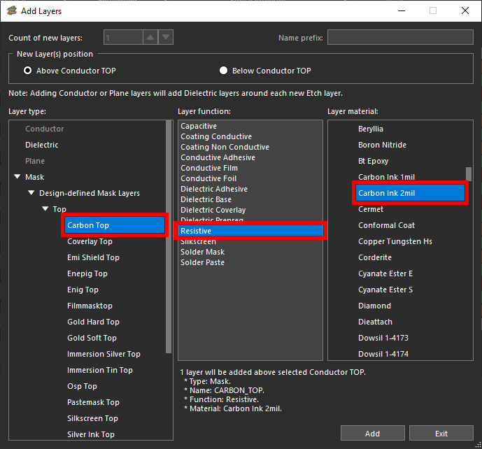
Step 7: Select Carbon Ink 2mil from the Layer Material list.
Step 8: Click Add. The top carbon layer is added to the stackup.
Note: Do not close the Add Layers window.
Defining a Silkscreen Layer
Step 9: Select Silkscreen Top as the Layer Type. Silkscreen is automatically selected as the Layer Function.
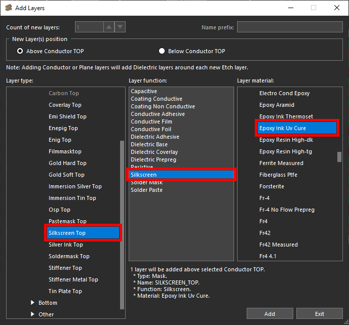
Step 10: Select Epoxy Ink UV Cure for the Layer Material and click Add.
Note: This material will be used as a place holder until a new material is created and assigned to the silkscreen layer.
Step 11: Click Exit to close the Add Layers window.
Step 12: Click Apply and OK to save the changes and close the Cross-Section editor.
Creating a New Material
Step 13: Select Setup > More > Materials from the menu to open the Material Editor.
Step 14: Right-click one of the listed materials and select Create New.
Note: The new material will be added to the bottom of the list.
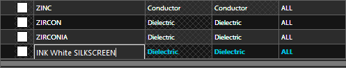
Step 15: Double-click the material name and enter INK White SILKSCREEN.
Step 16: Set the thickness to 0.02 mil.
Step 17: Click OK to save the changes and close the editor.
Note: All material data is stored in the file C:\Cadence\SPB_[version]\share\pcb\text\material.cmx.
Step 18: Select Setup > Cross-Section from the menu or the Cross-Section button from the toolbar.
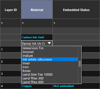
Step 19: Set the material for the silkscreen layer to the newly added Ink White Silkscreen layer.
Step 20: Click Apply and OK to save the changes and close the editor.
Wrap Up & Next Steps
Efficiently add resistive mask layers to your PCB design, such as conductive ink, to make design modifications and resolve errors with OrCAD PCB Designer. Test out this feature and more with a free trial of OrCAD and get more step-by-step instructions at EMA Academy.
