With today’s ever-changing and ever-more-compact designs, having the same schematic with multiple board form factors is not uncommon as different boards may be used for variant designs, different types of enclosures, and regional differences. In some cases, alternate footprints may be required to meet design specifications. OrCAD X Capture allows you to easily add alternate footprints to a component for efficient selection and multiple options during the PCB layout.
This quick how-to will provide step-by-step instructions on how to add alternate footprints to a component in OrCAD X Capture.
To follow along, download the provided files above the table of contents.
How-To Video
 Open in New Window
Placing Components with Multiple Footprints
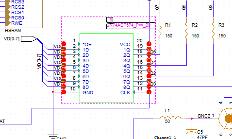
Step 1: Open the provided design in OrCAD X Capture. Double-click Release Root Schematic > Page 2 in the Project Manager to open the page.
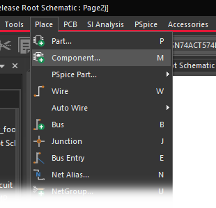
Step 2: Select Place > Component from the menu.
Step 3: The Component Explorer tab opens, showing a list of categories from which to search for components. Select Ultra Librarian.
Step 4: If prompted, enter your Cadence and Ultra Librarian credentials.
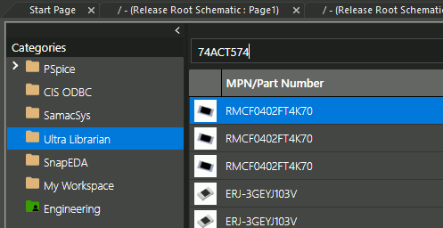
Step 5: Enter 74ACT574 into the Search field and press Enter.
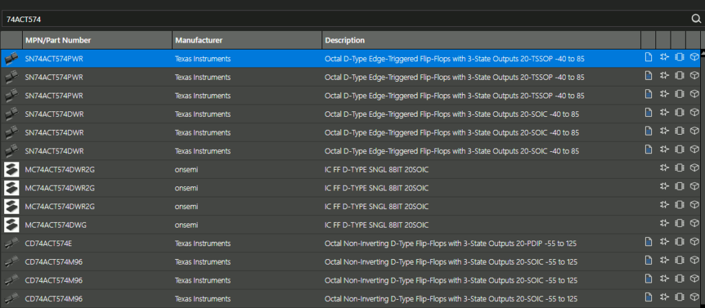
Step 6: View the results. Several instances of the component are listed in different packages and configurations.
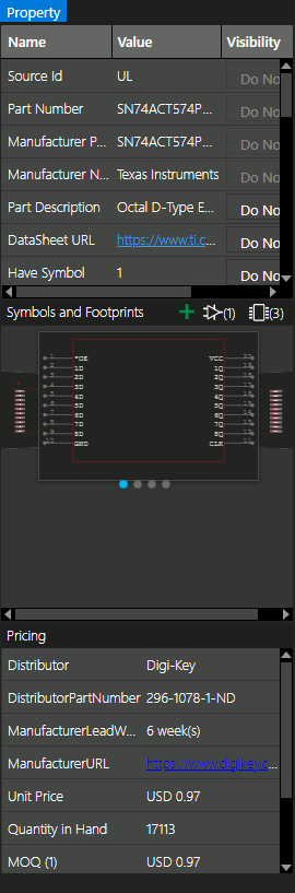
Step 7: Select the top listing of the component to view its properties as well as symbol and footprint in the Property tab. In this case, the component has three possible footprints associated with it.
Step 8: Right-click the component listing and select Place.
Step 9: Click to place the part in the empty space under Release Root Schematic > Page 2 in the Project Manager. Right-click and select End Mode or press Escape on the keyboard when finished.
Note: The reference designator is assigned automatically based on other components in the design. If the reference designator for this part is assigned as U8, skip ahead to Step 12.
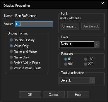
Step 10: Double-click the reference designator for the newly placed IC. The Display Properties window opens.
Step 11: Enter U8 for the value and click OK.
Step 12: Select the IC and press CTRL-C on the keyboard to copy.
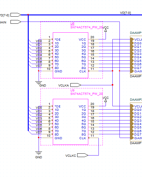
Step 13: In the Project Manager, double-click Data Schematic > Data Pg 1 to open the page in a new tab.
Step 14: Press CTRL-V on the keyboard to paste.
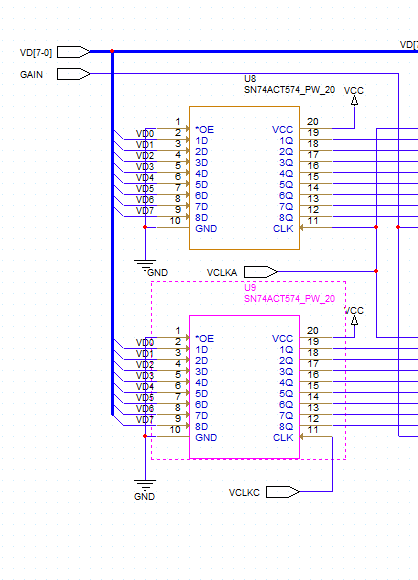
Step 15: Click to place an instance of the part in one of the empty spaces. Press CTRL-V on the keyboard again and place another instance of the part in the other space.
Note: Due to the hierarchical design, the reference designators may restart from U1. Since this design already has a part with reference designator U1, attempting to sync the schematic and PCB will throw an error. Perform the following steps to correct this.
Step 16: Double-click the reference designator for one of the chips. The Display Properties window opens.
Step 17: Enter U6 for the value and click OK.
Step 18: Double-click the reference designator for the other chip. Enter U9 for the value and click OK.
Step 19: Close the Component Explorer tab.
Checking Footprint Options
Note: Components placed from the Component Explorer with multiple footprints defined will download multiple footprint files.
Step 20: Open File Explorer and enter %home% into the filepath bar. This will browse to C:\Users\[username]\AppData\Roaming\SPB_Data.
Step 21: From there, browse to .\cdssetup\OrCAD_Capture\[version]\downloaded_parts\allegropcb. This folder contains a list of PCB footprints from downloaded parts.
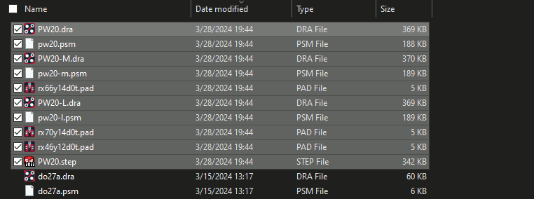
Step 22: Locate the most recently downloaded files. This chip has PW20 as its main PCB footprint and PW20-L & PW20-M as secondary footprints.
Step 23: Close File Explorer.
Add Alternate Footprints
Step 24: Back in OrCAD X Capture, select the Release Root Schematic: Page2 tab.
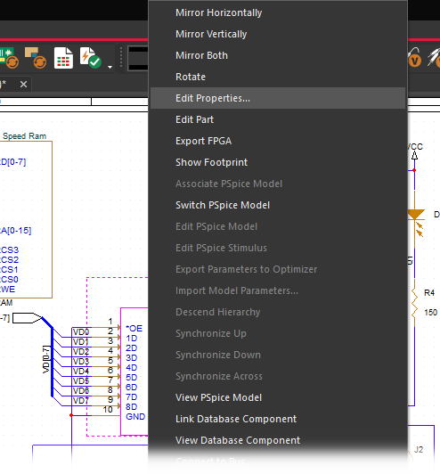
Step 25: Select the newly placed chip. Right-click and select Edit Properties.
Step 26: The Property Editor tab opens. Select New Property.
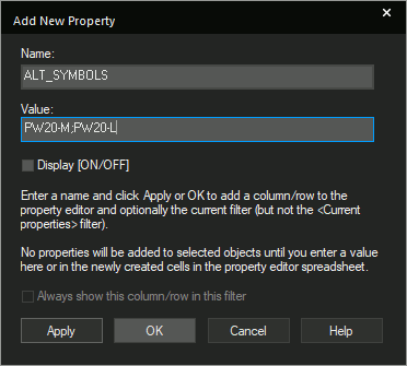
Step 27: In the Add New Property window, enter ALT_SYMBOLS for the name and PW20-M;PW20-L for the value to add alternate footprints for the component. Click OK.
Note: To only allow an alternate symbol on the top or bottom layer, enter T: or B: before the name respectively.
Step 28: Click Apply and close the Property Editor tab.
Step 29: Select the Data Schematic: Data Pg1 tab.
Step 30: Select IC U6. Hold CTRL on the keyboard and select U9. Right-click either IC and select Edit Properties.
Step 31: Select New Property. In the Add New Property window, enter ALT_SYMBOLS for the name and click OK.
Step 32: Right click on the ALT_SYMBOLS row and select Edit.
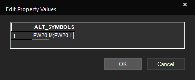
Step 33: Enter PW20-M;PW20-L and press Enter. The alternate symbols have been added to the properties.
Step 34: Click Apply and close the Property Editor tab.
Syncing the Changes to the PCB
Step 35: Select the .DSN file in the Project Hierarchy.
Step 36: Select File > Save from the menu to save the whole design. Select Yes to All if prompted.
Step 37: Select PCB > Update Layout from the menu.
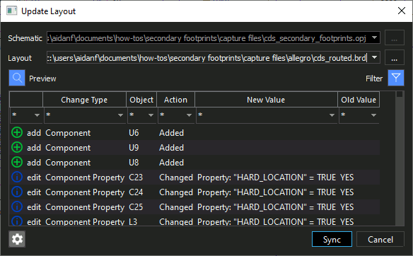
Step 38: The Update Layout window opens, showing the changes to be made. Click Sync.
Step 39: The Allegro Product Choices window opens. Select the appropriate license and click OK.
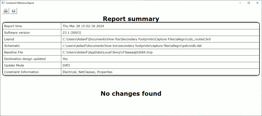
Step 40: OrCAD X Presto opens, showing a change report. View and close the report.
Step 41: Select File > Save from menu to save the changes. If prompted to overwrite the design, click Yes.
Confirming the Changes in OrCAD X Presto
Note: Changes can also be confirmed in OrCAD X PCB Designer as the process to add alternate footprints will implement secondary footprints for PCB layouts in either software package.
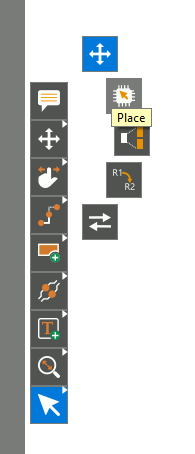
Step 42: Right-click the Move mode in the toolbar and select Place.
Step 43: Select Series in the Placement widget to place one component at a time.
Step 44: Select the hyperlink for Unplaced Components in the Properties panel. The list of unplaced components opens in the Search panel.
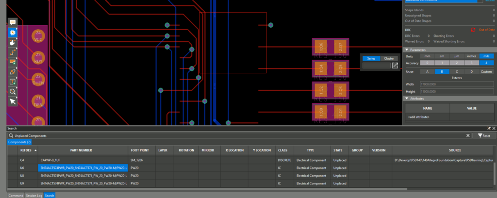
Step 45: Select U6, U8, or U9 from the list. A red rectangle appears in the canvas to indicate the placement boundary.
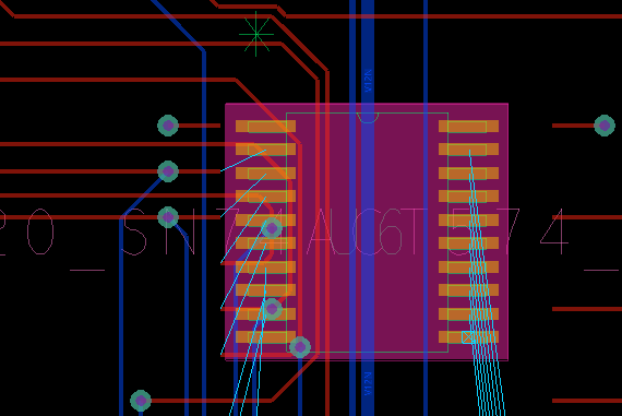
Step 46: Click to place the chip on the canvas. Press Escape on the keyboard when finished.
Step 47: Select the placed component.
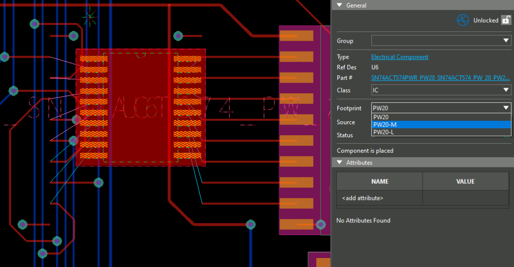
Step 48: In the Properties Panel under General, open the Footprint dropdown. The additional footprints are listed and can be assigned.
Wrap Up & Next Steps
Quickly add alternate footprints to components to efficiently accommodate design variants in OrCAD X Capture. Test out this feature and more with a free trial of OrCAD. Want to learn more about Capture? Get access to free how-tos, courses, and walk-throughs at EMA Academy.

