Impedance control is critical for high-speed PCB designs, RF, and mixed-signal applications to ensure proper functionality and reliable signals. Performing impedance analysis early in the design process can identify impedance discontinuities or mismatches during PCB creation, enabling you to correct errors early and minimize rework. Impedance analysis in OrCAD X Presto provides an efficient method to analyze impedance directly in the PCB canvas with:
- Easy to configure simulations
- Color-coded visual overlays
- Tabular results
- Cross-probing between simulation results and the PCB canvas
- Unified environment for design and analysis
This quick how-to will provide step-by-step instructions on how to perform impedance analysis in OrCAD X Presto.
To follow along, download the provided files above the table of contents.
How-To Video
 Open in New Window
Activating Impedance Analysis in OrCAD X Presto
Note: A separate installation is required to perform Impedance and Coupling analysis. For help configuring the installation and more information view the how-to here.
Step 1: Open the provided design in OrCAD X Presto.
Step 2: Select View > Panels > Analysis Workflows from the menu.
Step 3: In the Analysis panel, ensure the drop-down selection is configured as Impedance Analysis.
Note: OrCAD X Presto also includes Coupling analysis. For instructions on how to perform coupling analysis, view this how-to.
Performing Impedance Analysis in OrCAD X Presto
Step 4: Under Analysis Modes, select Net Based.
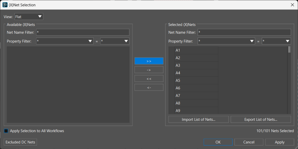
Step 5: Choose Select Nets.

Step 6: Click >> to select all the nets in the design for analysis then click OK.
Note: For more information on performing impedance analysis including, how to perform analysis using directed groups, view our free workshop here.
Step 7: Select Start Analysis. A progress bar displays the status of the simulation. When the analysis is complete a green check mark will appear next to Start Analysis.
Evaluating Impedance Analysis Results in OrCAD X Presto
Step 8: Under View Modes, ensure Net Based and Single Ended are selected.
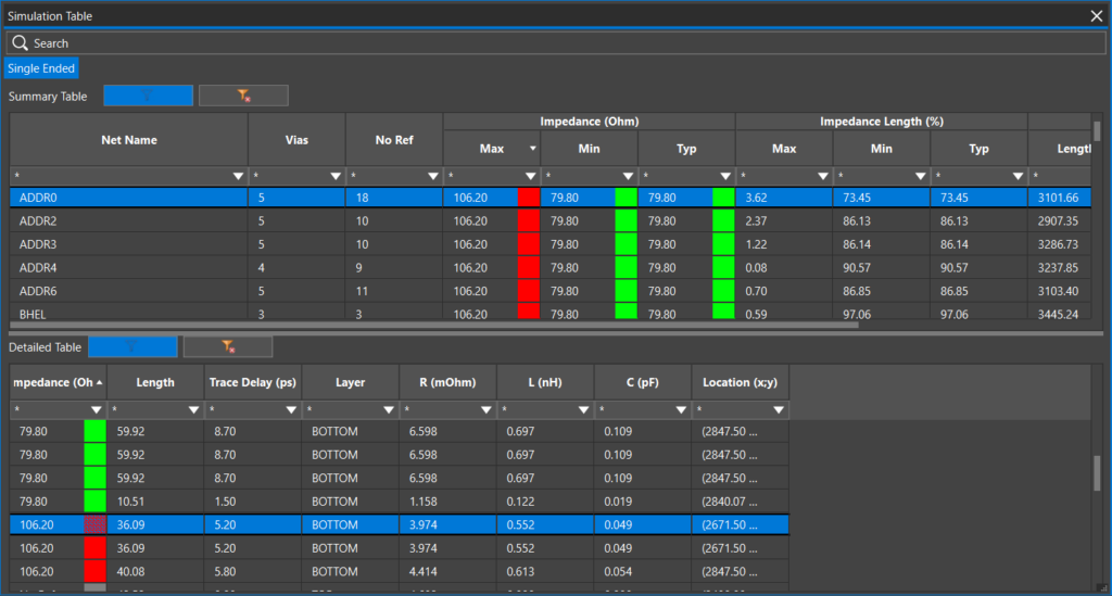
Step 9: Select View Impedance Tables. This provides tabular results including a summary of the impedance for nets in the design and detailed information. Impedance results are reported using a color-coded scale with blue being low impedance and red being high impedance.

Step 10: Select Max two times to sort the impedance results by the maximum values with the highest impedance values listed first.
Step 11: Select the ADDR0 net to view detailed information in the table below.
Step 12: In the detailed table, scroll down to the section of the net that is listed in red. Double click to be brought to the location in the PCB canvas and close the impedance table.
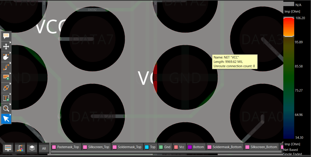
Step 13: In the Analysis panel, select View Impedance Visions.
Step 14: Slide the impedance bar up to filter the impedance vision to only high impedance nets.

Step 15: Hover around the identified impedance issue. Here you can see the trace is crossing an opening in the ground plane below. This impedance issue can be corrected by sliding the trace to move the trace away from the opening.
Correcting Impedance Issues in Your PCB Design
Step 16: Select View Impedance Visions again to turn off the impedance view in the PCB canvas.

Step 17: Select Slide from the toolbar.
Step 18: In the options, select Assisted and choose to Shove traces.
Step 19: Select the trace with the impedance issue and slide it to the left to resolve the error.
Step 20: Press Escape on the keyboard and choose the Select tool on the toolbar when finished.
Verifying the Effects of Design Modifications on Impedance
Step 21: In the Analysis Workflows panel, select Start Analysis.
Step 22: In the Save Analysis Results pop-up, select Ignore.
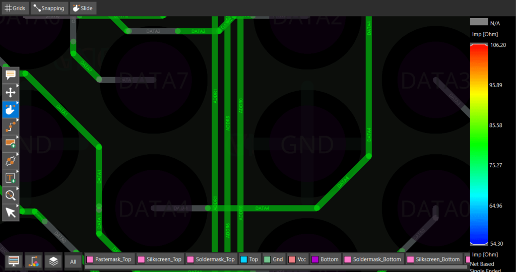
Step 23: When the analysis is complete, select View Impedance Visions.

Step 24: View the results. Moving the trace has corrected the impedance discontinuity. This process can be completed throughout the PCB design process to improve signal integrity.
Wrap Up & Next Steps
Efficiently analyze impedance during your PCB design process to improve signal integrity with impedance analysis in OrCAD X Presto. Get more step-by-step instructions for OrCAD X at EMA Academy.