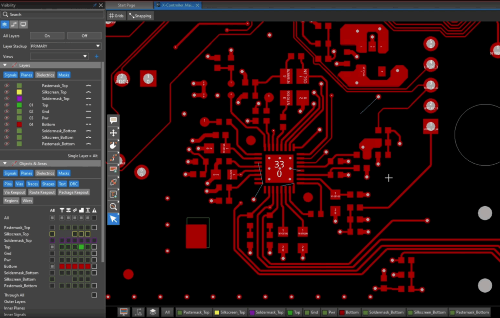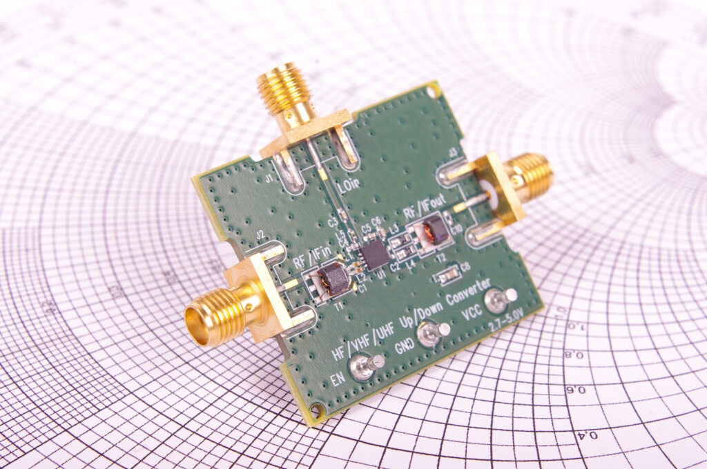
RF circuit design basics involve following a series of steps to minimize parasitics at high operational speeds, enabling the circuit to function effectively at frequencies extending into several GHz or beyond. These circuits are crucial for a range of applications, including wireless communication systems like Wi-Fi, Bluetooth, and cellular networks, as well as radar systems, satellite communications, and more.
Circuit design basics often aim to achieve a required power output in the baseband section while minimizing interference in the RF section, as these two sections of the circuit operate at different conditions.
Effective RF design requires precise impedance matching, extensive use of electromagnetic shielding, and consideration of high-frequency behaviors and parasitic influences. These elements ensure the stability and functionality of components —critical for maintaining optimal performance in RF applications.
RF Circuit Design Basic Blocks
Block Name | Description |
Oscillator | Provides a stable frequency source for various RF applications, crucial for synchronization in communication systems. |
Power Amplifier (PA) | Used to increase the amplitude of RF signals, essential in enhancing the strength of transmitted signals. |
Analog-to-Digital Converter (ADC) | Converts analog signals into digital data for processing, critical in digital communication systems. |
Filter | Constrains signal energy to specific frequency bands to prevent interference between radio signals. |
Local Oscillator (LO) | Provides the carrier frequency necessary for RF transmitters and receivers. |
Mixer | In transmitters, acts as an up-converter mixing low-frequency analog signals with LO to create RF signals; in receivers, serves as a down-converter. |
Low Noise Amplifier (LNA) | Amplifies faint signals, determining the sensitivity of a radio receiver. |
Transceiver | Combines both transmitting and receiving functions into a single component. |
RF Circuit Design Basic Steps
- Start by developing a comprehensive specification for the design, detailing functions and key parameters. This includes the required gain and noise figure of the Low Noise Amplifier (LNA), the output power of the Power Amplifier (PA), the phase noise of the Local Oscillator (LO), and the conversion gain of the mixer.
- Next, create a block diagram at the device level, utilizing components as required —anything from oscillators, mixers, and filters.
- Then, verify that the design meets the specified requirements through circuit simulation. This includes modeling variations in the manufacturing process and operational conditions to ensure the circuit behaves as intended.
- Next, implement the layout of the design by arranging the layouts of all blocks and associated components based on signal types. Follow specific placement rules to ensure the design is manufacturable.
- Finally, extract the equivalent circuit from the layout. At this stage, parasitic effects become part of the design description. Re-simulate the design to confirm it still performs as intended, even with the addition of these parasitic effects.
Stackup Basics
It’s important to design your PCB stackup before developing your RF circuits, particularly passive ones, as they depend on achieving specific impedance targets for proper functionality. Design the RF circuit PCB stackup to ensure it provides the desired impedance characteristics for the RF components. The stackup should be configured so that RF elements maintain their required characteristic impedance. However, the overall impedance of your system will also depend heavily on the layout and routing of your RF circuit.
Material Selection
Material selection for the PCB significantly affects circuit performance at high frequencies.
- For frequencies beyond Wi-Fi (~6 GHz), PTFE or thermoset polymer materials are generally preferred over FR4 due to their superior performance in supporting RF signal propagation and printed RF circuit designs.
- FR4 materials, composed of resin-filled fiberglass weaves, can still be used for RF transmission lines and interconnect at frequencies up to Wi-Fi levels.
- At higher frequencies or for very long interconnects, PTFE-based laminates and bondply materials are recommended. These materials have a lower loss tangent than FR4, allowing signals to travel farther without significant attenuation.
RF Trace Impedance
Printed RF circuit designs also leverage the propagation of electromagnetic fields along transmission lines, which is influenced by the dielectric properties of the substrate material. Determine the width of the conductors on the PCB to achieve the desired impedance, typically 50 Ohms, in your designs. The relationship between the impedance of a trace and its dimensions can be calculated using formulas through conformal mapping.
As discussed above, high-speed circuit design requires augmenting electronic circuit design essentials with RF circuit design basics to ensure functionality, signal integrity, EMI/EMC compliance and performance objectives are met. This is achievable by employing effective RF simulation tools. For optimization, it is best to partner with a PCB design software provider that can help you select the right program for your application and implement it most efficiently.
EMA Design Automation is a leading provider of the resources that engineers rely on to accelerate innovation. We provide solutions that include PCB design and analysis packages, custom integration software, engineering expertise, and a comprehensive academy of learning and training materials, which enable you to create more efficiently. For more information on RF circuit design basics and how we can help you or your team innovate faster, contact us.


