 Designers can sometimes miss the forest for the trees when routing: while continuity according to the netlist is the overarching goal, failing to heed typical signal integrity conflicts results in a “completed” board that fails expensive electromagnetic compatibility (EMC) testing. Some ad-hoc corrections at the board/enclosure level can paper over minor electromagnetic interference (EMI) issues. Still, the best course of action is almost universally a board redesign to counter EMI at the source. The good thing to note is that signal integrity problems and solutions are generally straightforward, either using data-driven analysis of a prototype board or time-honored approaches.
Analyzing Signal Integrity Problems and Solutions | ||
Symptom(s) | Cause(s) | Solution(s) |
Reflection | Stubs, impedance mismatches | Stub removal (e.g., backdrilling), matching impedances |
Metastability | Power delivery network (PDN) issues | Evaluation of decoupling capacitors (placement/value) |
Crosstalk | Long sections of parallel traces, close placement to EMI-aggressive components | Greater trace spacing (inter- or intra-planar), reorganizing routing to avoid components |
Where Poor Signal Integrity Manifests
Signal integrity always starts at the design, but test engineers often diagnose symptomatically from the assembled board. Signal integrity issues occur in the analog and digital realms:
Digital Signal Integrity Problems
- Bus contention – When multiple drivers attempt to drive a bus concurrently (e.g., one or more of the signals do not enter a high-impedance state to block transmission), the combination of signals can cause bit errors if the bus does not reach its voltage threshold.
- Metastability – Signals that fall between or outside logic level thresholds can produce runtime errors like late transceiving, producing further bit errors.
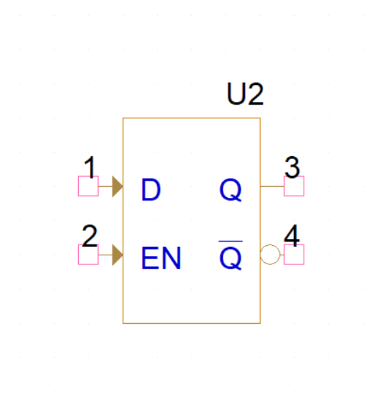
- Setup and Hold violations – Clocked devices (e.g., a flip-flop) require data to arrive at a certain point before and after the clock signal arrives (hence setup and hold). When data arrives in an unstable state or does not adhere to the setup-and-hold requirements, the output can change drastically relative to expectations. With digital devices’ increasing rise/fall time to support faster processing, setup-and-hold requirements are becoming more strict.
- Undefined conditions – When multiple data inputs have unaligned switching states, the timing difference produces an incorrect output relative to the design. The mismatched switching times are sometimes due to variations in the signal pathing (length, return path, etc.).
Analog Signal Deviations
- Amplitude errors – Signals can oscillate about their targeted levels, producing inconsistent results and states. Droop or runt amplitude levels can fail to trigger threshold levels promptly (or at all).
- Crosstalk – Parallel signals routed nearby can couple capacitively and inductively. The more dominant signal characteristics can drown out the more susceptible signal line and create excessive noise. As signal speeds increase, the potential and intensity of the inductive coupling also increases.
- Ground bounce – Ground bounce (alternatively, supply bounce) is partially unavoidable; it mainly stems from package design, and the designer has little opportunity to mitigate this value. When current inrushes or outrushes on signal lines during a state transition, the local voltage can fall below the voltage rail or exceed the ground voltage. Either of these conditions can produce indeterminate logic states and runtime errors.
- Jitter – Clocked circuits depend on the signal’s leading/lagging edge to trigger consistently across periods. Variations in the edge placement (owing to noise or crosstalk) can desynchronize circuit functions tied to the same clock.
- Reflections – When improperly terminated, some energy of the transmitted signal travels back to its origin point. Not only can the lost energy at the receiver affect performance, but the reflected signal can now destructively interfere with the next incoming pulse.
- Signal-edge transitions – Poor board layouts or improper termination at the receiver can cause signal rounding, leading to delayed transition states while the signal reaches threshold voltage.
Signal Integrity Problems and Solutions
Since engineers typically diagnose EMI during laboratory testing, correcting it becomes an expensive proposition. Fortunately for EMI management/EMC design, many issues are mitigable during layout with proper foresight. Staying mindful of these potential EMI causes can prevent unnecessary redesigns and reduce design turnaround times:
- Clock distribution – Clock lines should receive priority during routing; avoid routing too close to highly inductive elements whose current-switching can couple to the clock signal. Ensure a consistent plane reference across the travel path and reduce the clock signal trace lengths whenever possible. Timing devices pre-receiver can “clean up” the clock signal to minimize jitter.
- Decoupling – Decoupling capacitors pass DC signals while shunting AC signals to ground. Designers distribute decoupling capacitors throughout the design to filter the power signal and discharge stored energy when the system power draw is high to prevent voltage sags. Careful placement of decoupling capacitors keeps equivalent series inductance low.
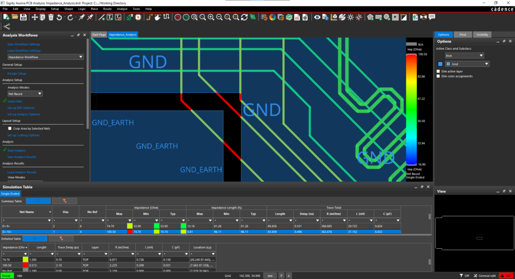
- Impedance and loading – Impedance matching sources and loads prevents signal reflections.
- Noise margin – Logic high and low thresholds differ depending on the package’s logic; for example, CMOS technology has a greater noise margin than TTL because the former’s high-logic threshold is closer to the supply voltage, and the low-logic threshold is closer to ground.
- Return currents – Current must flow in a loop; for single-ended traces, designers must account for the return current that must flow from the routed destination to the origin. A continuous, unbroken reference plane without gaps (i.e., no split-plane crossing) will offer a direct, low-impedance return path.
- Signal paths – Avoid crosstalk by appropriately spacing traces and avoiding long parallel sections. Be conscious of coupling on adjacent signal layers as well. Do not route signals close to switched-mode power supplies due to the potential for inductive coupling.
- Stubs – A stub is an additional (intentional or unintentional) portion of the signal transmission line. It can produce reflections depending on its length relative to the signal’s wavelength and the parallelity to the transmission line. However, it can be a beneficial tool in RF PCB design for impedance matching.
EMA Design Automation Assists PCB Design Workflows
Signal integrity problems and solutions require a mindful approach to PCB layout that evaluates signal paths for EMI. For design teams, knowing where and what to look for can be the first challenge to overcome. However, design teams don’t have to go it alone: from top analysis software to design support (up to complete layout services), EMA Design Automation ensures that devices can meet the stringent requirements of EMC field operations.
EMA Design Automation is a leading provider of the resources that engineers rely on to accelerate innovation. We provide solutions that include PCB design and analysis packages, custom integration software, engineering expertise, and a comprehensive academy of learning and training materials, which enable you to create more efficiently. For more information on PCB design documentation and how we can help you or your team innovate faster, contact us.


