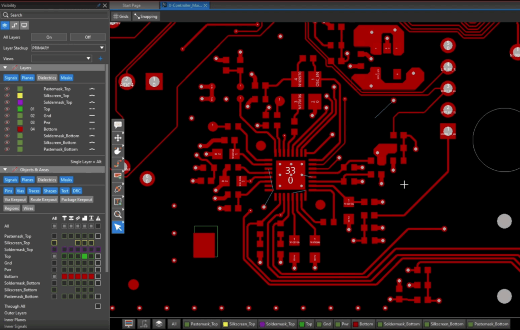
Signal Integrity Analysis in PCB Design: Need for Accurate CAD Models
Signal integrity analysis requires accurate CAD models and part information because they provide precise physical and electrical characteristics of components, which affects the behavior of high-speed signals. Inaccuracies in component dimensions, materials, or layout can lead to incorrect simulations, resulting in signal reflections, crosstalk, or electromagnetic interference (EMI) issues. Below is a table outlining the importance of having accurate CAD models and part information for signal integrity analysis:| Signal Integrity Analysis: Importance of Accurate CAD Models and Parts Data | |
| Aspect | Importance to Signal Integrity |
| Component Dimensions | Precise component dimensions ensure the physical layout matches the electrical design, reducing signal reflections or crosstalk issues. |
| Electrical Properties | Accurate component electrical characteristics (e.g., impedance, capacitance, inductance) are critical for minimizing signal degradation. |
| Pin Configurations | Correct pin assignments and spacing ensure proper connections and avoid signal integrity problems like ground bounce. |
| Material Properties | Knowing the exact material properties helps calculate propagation delays and signal attenuation. |
| Trace and Via Geometry | Correct CAD models enable accurate trace width, via size, and spacing, critical for maintaining consistent impedance and signal quality. |
| Connector Models | Accurate connector designs help reduce impedance discontinuities, essential for high-speed signals to prevent reflections and signal loss. |
| Thermal Considerations | Thermal properties derived from CAD models can predict heating effects, which affect signal integrity due to changes in resistance and impedance. |
| Layer Stackup Information | Precise layer stackup data (including copper thickness and dielectric spacing) ensures proper impedance control for signal traces, especially for high-speed designs. |
| PCB Layout and Routing | Accurate CAD models help optimize routing strategies to minimize crosstalk, signal skew, and interference, key for signal integrity. |
| Mounting and Packaging Details | Correct physical models allow proper mounting and packaging, avoiding EMI, which can degrade signal quality. |
Signal Integrity Analysis Tool and Techniques
Selecting a top signal integrity (SI) analysis tool is crucial in PCB design, especially as modern electronics increasingly require high-speed data transmission and complex multilayer boards. These tools help engineers identify and resolve issues like signal distortion, crosstalk, impedance mismatches, and timing errors that can severely affect the performance and reliability of a design. Signal analysis tool capabilities and functionality can vary significantly. Consequently, it is important to choose tools that will integrate well with your ECAD software and CAD model formats. Below is a list of signal integrity (SI) analysis tools for PCB design, along with distinguishing attributes that are helpful when searching for a match for your project.- Cadence Sigrity: Comprehensive SI, power integrity (PI), and EMI analysis, with support for multi-gigabit signal channels.
- Ansys HFSS: High-frequency 3D electromagnetic simulation for detailed SI analysis, impedance matching, crosstalk, and EMI/EMC effects.
- HyperLynx SI: Intuitive SI and PI analysis with high-speed design verification, including timing analysis, crosstalk, and reflection analysis.
- Keysight ADS: High-speed digital SI analysis tool, with channel simulation, jitter, and bit error rate analysis.
- ANSYS SIwave: SI and PI analysis for PCBs and IC packages, with accurate DC voltage drop, timing, and electromagnetic field simulation.
- SiSoft QSI: Quantum SI, now part of Keysight, focuses on high-speed serial interfaces with SI, jitter, and crosstalk analysis in multi-gigabit channels.
- Simberian Simbeor: Modeling and simulation of interconnects and PCB materials for high-speed designs, focusing on accurate signal transmission and SI performance.
- Zuken CR-8000: Integrated design suite with SI, PI, and EMI/EMC analysis for complex, multilayer PCB designs with high data rates.
- Polar Instruments SI8000: Impedance control and analysis for PCB trace matching, critical for maintaining SI across high-speed transmission lines.
- Xpeedic SI: Fast SI simulation, focusing on interconnects, power delivery network analysis, and multilayer PCB designs in high-frequency environments.
- SigXplorer (Altium): SI analysis tools to check impedance, signal quality, and trace crosstalk in PCB layouts.
- Mentor Graphics Xpedition: Advanced SI analysis, including channel simulations, ensuring design rule compliance in high-speed digital designs.
EMA Design Automation is a leading provider of the resources engineers rely on to accelerate innovation. We provide PCB design and analysis packages, custom integration software, engineering expertise, and a comprehensive academy of learning and training materials. For more information on signal integrity analysis in PCB design and how we can help you or your team innovate faster, contact us.


