I hate unclear schematics. I know engineers are extremely smart, but they tend to fall short when it comes to clearly conveying their design ideas and requirements. When I see a schematic missing block diagrams, sectioned off areas, and lacking clear notes (which is practically all schematics I’ve seen), I want to throw my coffee and computer out the window.
The Problem with a lot of Schematics
They’re unclear. I should be able to read through a schematic and understand the full story of the design from start to finish without necessarily having to perform pen and paper calculations. As I type this article, I am using KVL and KCL to back-calculate what goes where in a current design in relation to a previous PCB (and to the project overall).
This backwards approach to decipher a previous designer’s work, while intellectually stimulating, defeats the purpose of making the schematic in the first place; to help the designer and other engineers understand what’s going on without redoing the design themselves.
We as engineers often focus on having our schematics make sense to us and be able to explain the design to other stakeholders, but I think we can go beyond that. I believe there is an ideal schematic; the kind that leaves the engineer more aware of a design, rather than confused.
The Ideal Schematic
Let’s understand the true purpose of the schematic, by my definition, which is to communicate the design intent in its entirety: physical limitations, thermal considerations, functionality, electrical characteristics, what the final PCB should look like, etc. The flow of the design should, at minimum, loosely follow the flow of operation from power to final output.
Let’s rebuild the schematic from the ground up and create the gold standard for designing schematics everyone will enjoy reading.
Absolute minimum building blocks for a schematic
The purpose of the schematic is to communicate an idea. For communication to be effective, it needs to be clear. Ultimately, this rests on the schematic creator, not the one reading it.
While not every element in the following list is necessary for a schematic to make sense, ideally for me, every schematic would have the following properties:
- Cover Page
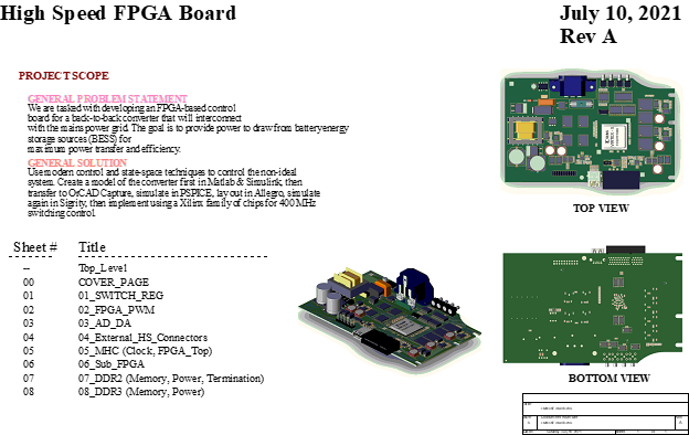
Just like the cover of a book, a cover page for the schematic immediately gives an idea of the content inside. The table of contents allows engineers to easily navigate the contents of the schematic. For a complete cover page, include a table of contents, description of pages with page numbers, and an image of final PCB or final PCB intent. A lot of people, especially clients PCBs are designed for, like to know what the end product will look like upfront. This will make it so much easier for someone to immediately understand the scope of the product and get an idea of the final product.
- Project Statement
While the cover page gives the overall idea of the product, we need specifics on the purpose of the project, goals, targets, and anything else the cover page does not convey. Whenever there is a discrepancy about what is supposed to be worked on in the project, you can always refer to the project statement in the schematic. The project statement is useful for hardware test engineers, electrical design engineers, and practically any stakeholder in the project. This also keeps everyone on the same page and ensures nobody wastes time doing tasks not beneficial to the project.
Placing the scope, intent, and requirements of the project in the schematic eliminates the need for a separate document to understand what needs to get done. The scope can be compiled from any project statements defined in your project management system or notes. Finally, a high-level understanding of the project makes reading the rest of the schematic so much easier. While mysteries are fun to solve, I don’t want to waste time trying to understand the purpose of the project when I’m supposed to redesign a schematic with hair pin accuracy and 100% comprehension.
- System Block Diagram
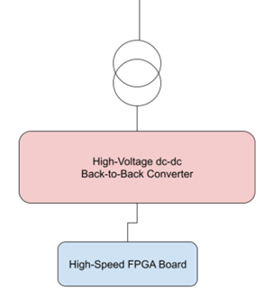
Now that we understand the intent and scope of the project, let’s focus on how we’re going to achieve the goals set in the project statement. This is where a good system block diagram comes into play. Include a system block diagram that explains the features, functions, and modules needed to make the desired product and the end goal possible.
Pro Tip: Put high level notes on requirements into the blocks.
- Functional Block Diagram
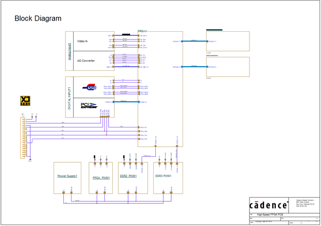
High-speed FPGA Board
Depending on the complexity of the design, the system block diagram and functional block diagram could be one in the same; however, the differences are somewhat nuanced. For instance, the system block diagram might include devices or objects in the environment surrounding the main product and the outside cables that connect to it. The functional block diagram is limited to the product only.
The functional block diagram is a lower-level block diagram that shows how each major block in the system will achieve the required functionality. It shows the main signals in the design, possible external sources (like critical signals from programming code), and critical voltage and current requirements.
- Electronic Component Schematics of Each Functional Block
Next we need circuit diagrams (schematics) that will actually achieve what was defined in the function blocks. Once we know the circuits and the components that make them, we can go search for those electronic parts and buy them to build the project. This is the point where we can start pricing and budgeting for real design costs. Once we know the parts, we know the prices, and can get reasonably close estimates on board prices before we even design a printed circuit board.
- Standard Consistent Reference Designators
If we place parts on the design without a consistent way to refer to them, understanding the schematic could get annoying at best or a complete nightmare at worst. Hence we use standard Alpha-numeric reference designators that quickly give us an idea of the types of devices placed on the schematic. So instead of having to look up every other part, the reference designators help us quickly interpret the schematic without stopping.
- Mechanical/Other Components and Devices
Hardware products often include both electrical and mechanical devices that may or may not be part of the board itself, but are required for the final product. We want to avoid mishaps where we get the PCB delivered, but can’t mount the PCB into an enclosure or forget the enclosure altogether. Therefore, we need to keep a record of all parts for the full project. Now putting them in a high-level document or within the PCB documentation is great, but I can’t think of any place better than on the schematic itself.
- Accurate Parts Library
In the words of Tom Hausherr, primary author of IPC-7351B and owner of PCB libraries.com, “PCB Design perfection starts in the CAD library”. On the flip side, the most time consuming problems I’ve ever faced in designing PCBs are discrepancies with symbols and footprints. Getting footprints and part numbers wrong, when I’ve already delivered the design to the manufacturer, always results in a redo that could take hours to fix. In my case when working on a project for one of my clients, getting a few part numbers and footprints wrong held me up for a full week and a half.
All parts contain manufacturer part information, PCB land patterns, and functional pins on the parts (e.g. pins are ordered according to how they are on the physical device in real life). Spend time creating the parts properly upfront and verify all information is correct. The upfront work and due diligence will make BOM and PCB creation so much smoother.
- Change Notes and Revision Notes
At one of my previous jobs, design changes happened so frequently, much of our engineering team would get confused between design releases. This caused us to rely heavily on the design revisions and notes to stay on track. Utilize as many notes and revision notes in your design as possible. Doing so will clear up a lot of questions before they are even asked. Having a good set of notes helps us find the differences in designs and critical parts more quickly.
- Title Block
Including a title block helps to always know which part of the schematic we are looking at as well as the name of the project. It also looks more professional to have a title block. Be sure to include the name of the designer, the company, the date the document was created, modification date, and of course, the design name and specific schematic sheet.
General Rules to Follow When Creating a Schematic
The purpose of communication is to transmit an idea from one medium to another and the purpose of a schematic is to communicate your design intent. In order for this to happen, the communication needs to be easy to follow, clear, and transparent. This means the design needs to be logical, consistent in its presentation, and have a ton of notes.
Create a Logical Flow
- Have signals flowing from left to right: inputs on the left and outputs on the right. This style is applicable on both high-level drawings or for each individual part/module.
- Break the schematic into multiple sheets based on circuit functionality.
- If appropriate, make the schematic hierarchical and integrate into a high-level interactive schematic version of your system block diagram.
- Place similar kinds of circuits together based on functionality. For example, place power circuits on the same page/area, place analog circuitry in the same page/area, and likewise for digital circuitry. This prevents stakeholders from looking all over the schematic just to find the different power supplies.
- Place bypass and decoupling capacitors in their own groups.
- Use pull-up or pull-down resistors wherever appropriate.
- If applicable, add graphics that show some relation between a circuit section and the physical object it needs to control or be a part of. This needs to be incorporated even if it’s part of an older version of the PCB.
Create Consistency and Improve Readability
- Use standardized schematic symbols from ASME Y14.44-2008 and IEEE 315-1975. Luckily practically all ECAD software tools have these standard symbols already.
- Utilize an accurate part library: Make sure pin numbers on the schematic symbols match the physical part and PCB footprint.
- Consistently orient symbols (either horizontal OR vertical).
- Name all nets.
- For discrete components (resistors, capacitors, diodes, inductors, etc.) include the value, voltage and current operation, and symbol footprint size code if applicable (0603, 0402, etc.).
- Properly label all the different types of ground references in the design (power ground, signal ground) and make sure they have distinctly different symbols for each type.
Add Notes to Clearly Communicate your Design Intent
- Explain any off-board signals that are on the schematic. This can be included in a legend in the corner of the drawing or at the end of the schematic pages.
- For unidirectional part symbols, consider information which may need to be added to the symbol to prevent the part from being installed backwards.
- Critical Information (High voltage and High current).
- Indicate the original/source sheet number for the ports on the schematic.
Funny story: In one of my previous roles and during my experience testing electronics, I had printouts of the circuit schematics practically glued to my fingers while I checked every pin on the design. Even then, one ambiguously drawn part on the schematic for power (that always seems to be the case, the most critical part of the schematic) had no notes on it. Rest assured our team flipped the power connector backwards, because of course it was not a keyed connector (it’s wise to use keyed power connectors), and risked damaging the system/board. Luckily the electronics designer put a reverse blocking diode to prevent that problem from happening. If he hadn’t put in that diode, we might have caused some slight board damage to a special $9000 inverter. While good schematics were helpful, I wish we had tools like inspectAR so I wouldn’t have to carry around schematics. Would have saved me so much time and headache, but I digress.
- Add trace width for traces carrying a lot of current.
- Identify length matching for high-speed lines.
- Indicate traces that need controlled impedance.
- Specify resistor purpose (pull-up/pull-down resistors)
- Note capacitor placement (close to the supply pins on microcontrollers or processors)
- Note intentional part placement. This really helps PCB layout engineers save some time from having to look in the data sheet to see which capacitors you used are supposed to put close to the device.
Keep this printable checklist on hand to easily implement these guidelines into your design process.
Will These Schematic Tips Help Other Engineers?
As engineers, we’re becoming busier every day; therefore, anything to help us do our jobs faster is important. The schematic holds the entire product design together, making it a key design tool. The ability for both the engineer and other stakeholders to understand the schematic completely is critical and quite near mandatory. With a complete schematic, there will be fewer questions and mistakes when other engineers need to rework, modify, or reuse the design. PCB layout engineers will have a much easier time placing parts and wires in optimal positions for layout. Testing can be performed quickly without as many hiccups from poorly done schematics, saving time and frustration. Treating your schematics like a standalone PowerPoint presentation will effectively communicate design intent, eliminating preventable errors. Simply put, great schematics save time and who wouldn’t benefit from that?
