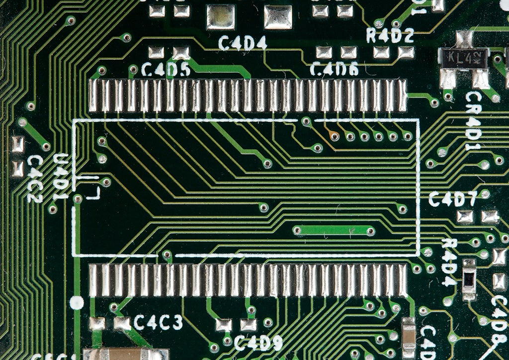
Connecting all of the various nets of a PCB layout can seem to the untrained eye like playing a massive game of Connect the Dots: users draw lines from points without overlapping to realize the logic of the schematic. Individually, these connections represent direct communication between two points, but in the context of the greater network, the groupings of these connections can significantly affect device speed and performance. Routing topology in PCB design can range from relatively simple to moderately complex, with different methods yielding performance tradeoffs that make them best suited for particular applications, memory formats, and architectures.
Common PCB Routing Topologies
Routing topologies for circuit board traces vary and require an understanding of routing best practices. However, there are several routing scheme implementations that PCB designers commonly deploy. The best selection is made by understanding the advantages and disadvantages of these options, as listed below.
Investigating Routing Topology in PCB Design
Point-to-Point
The most straightforward connection has a single link between unique same-net pads/vias. The signal travels from one end to the other without any redirect or intermediary. Point-to-point (P2P) connections are easy to implement and benefit from the shortest, most direct connection for low-impedance communications. Troubleshooting P2P is a rapid process as only two net objects are involved with transceiving. However, the simplicity of P2P means low redundancy, as no alternate signal paths exist if the connection fails.
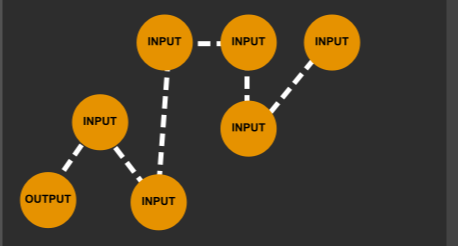
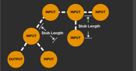
Daisy Chain
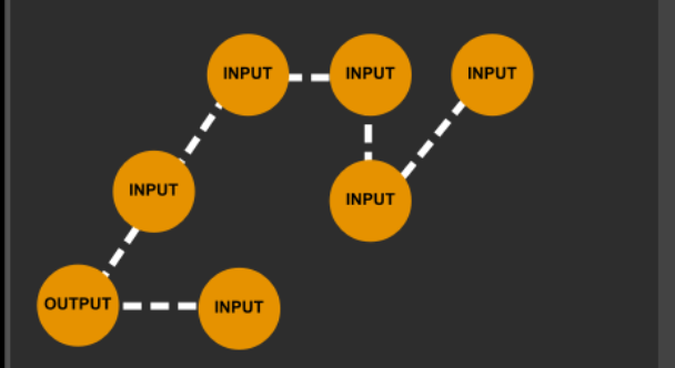
A daisy chain is multiple, sequential point-to-point connections (i.e., three or more same-net pads/vias). Unlike in P2P, a daisy-chained topology may only require partial traversal to reach its target destination. Because there are more interfaces the signal encounters, signal reflection becomes more pronounced relative to P2P. However, the combination of direct routing between multiple same-net pads/vias helps reduce stubs and stub length, which can also cause reflections or form antennae.
A daisy chain can wrap back around itself from the first and last same-net vias/pads to transform into a ring. The ring is more redundant since it can accommodate at least one connection failure, which turns it back into a linear daisy chain (described above). Additionally, the ring can reduce topology traversal time by cutting the signal pathing in half; instead of traversing end-to-end, a signal entering the ring can choose the shortest “halfway” route. Note that this is half of the topology distance – a signal may encounter a longer physical transmission half-path, depending on the layout.
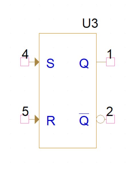
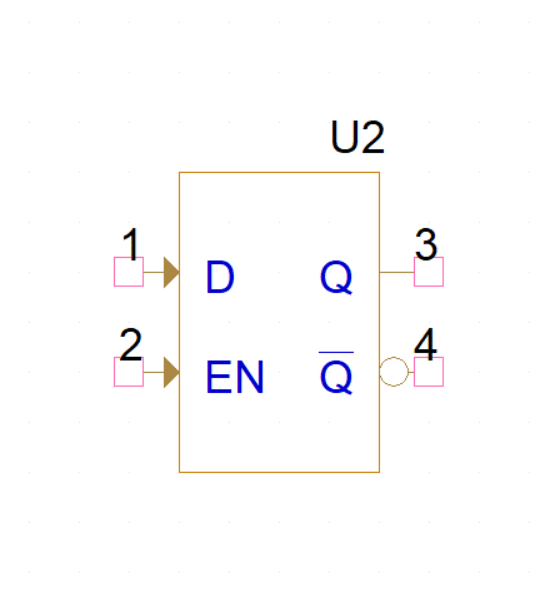
Source Load Daisy Chain
For Source Load Daisy-Chain, it is important to note the serial electrical topology restricts the elements to the same electrical capacities, as shown below.
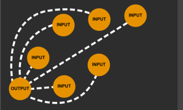
Bus
A bus is a common signal dissemination topology that uses a signal “backbone” (or “trunk” in a tree topology) to distribute the signal to all of the same net pads/vias simultaneously. Signal transceiving is always one step away in the bus topology: from bus to endpoint or vice versa. To avoid interference between the various nodes of the network, bus signal transmission includes an address that indicates whether the node should act upon or ignore the signal reception. The bus topology is exceptionally cost-effective and highly amenable to future expansion since each new node integration requires only the connection to the bus. However, redundancy is low since a failure anywhere along the bus connection disrupts signal transmission. Layout designers must be mindful of the length of the bus connections to manage stub lengths and avoid quarter-length wavelengths that can maximize reflections.
The standard bus topology is a linear bus with terminations at the end nodes to prevent signal reflection. Combining a bus and daisy-chain topology for a distributed bus is possible—the distributed bus functions identically to the linear bus topology.
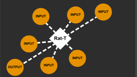
Star
The star topology relies on a central same-net pad/via that acts as the intermediary between all outlying nodes for signal transceiving. It is like a bus but with a central node rather than a central connection. Due to its similarities in topology, the star shares many of the advantages and disadvantages of the bus. Implementation is easy as each new node only needs to connect to the central node, but the central node represents a single point of failure. The central node can also struggle with bandwidth issues when the number of outlying nodes is significant.
Mesh
A mesh is similar to a ring topology in structure but contains additional connections between nodes that bolster topology traversal and redundancy. A full mesh has every node connected to every other node – this arrangement offers the fastest topology traversal (each node is one step away from every other node). However, implementation can become extremely cost-prohibitive as the number of nodes increases. A partial mesh is a compromise between topology traversal and connection count. Designers can add connections between highly trafficked nodes to improve transceiving while leaving less trafficked nodes toward the edges of the ring/daisy chain where they are still accessible (albeit with a longer topology traversal).
Minimum Spanning Tree
When using minimum spanning tree, it is important to define stub length constraints to maximize signal integrity and ensure acceptable impedance levels are maintained.
Far End Cluster
Far end cluster routing also seeks to maximize signal integrity by minimizing or restricting the length between receivers, which is exhibited below.
How to Optimize Your PCB Routing Process
The best way to route your board efficiently is to effectively organize your constraints based on the routing topology selected. Routing topology in PCB design can use any single or combination of the described networks above to optimize signal transceiving within the board layout. Yet, the routing process can be tedious and filled with back and forth between routing traces and correcting violations. Implementing routing topology in PCB design depends on knowing the various schemes and utilizing the software tools that enable you to leverage the best method for your design.
As with all aspects of PCB design, the degree of workflow efficiency and optimization depends upon the software tool employed and its capabilities. For industry leading layout software, OrCAD X, the following routing topology options are available.
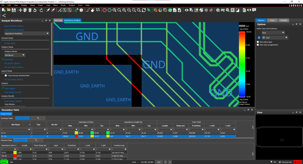
OrCAD X Routing Topology Options
Making the best use of routing topology options and integrating them with other functionality, such as autorouting, is the mandate to lay out your board most efficiently. Satisfying these requirements often necessitates partnering with an industry leader in helping engineers maximize innovation and development by providing the best EDA design and routing tools, custom integration programs and comprehensive training and support resources.
EMA Design Automation is a leading provider of the resources that engineers rely on to accelerate innovation. We provide solutions that include PCB design and analysis packages, custom integration software, engineering expertise, and a comprehensive academy of learning and training materials, which enable you to create more efficiently. For more information on how to best incorporate PCB design layout guidelines and how we can help you or your team innovate faster, contact us.