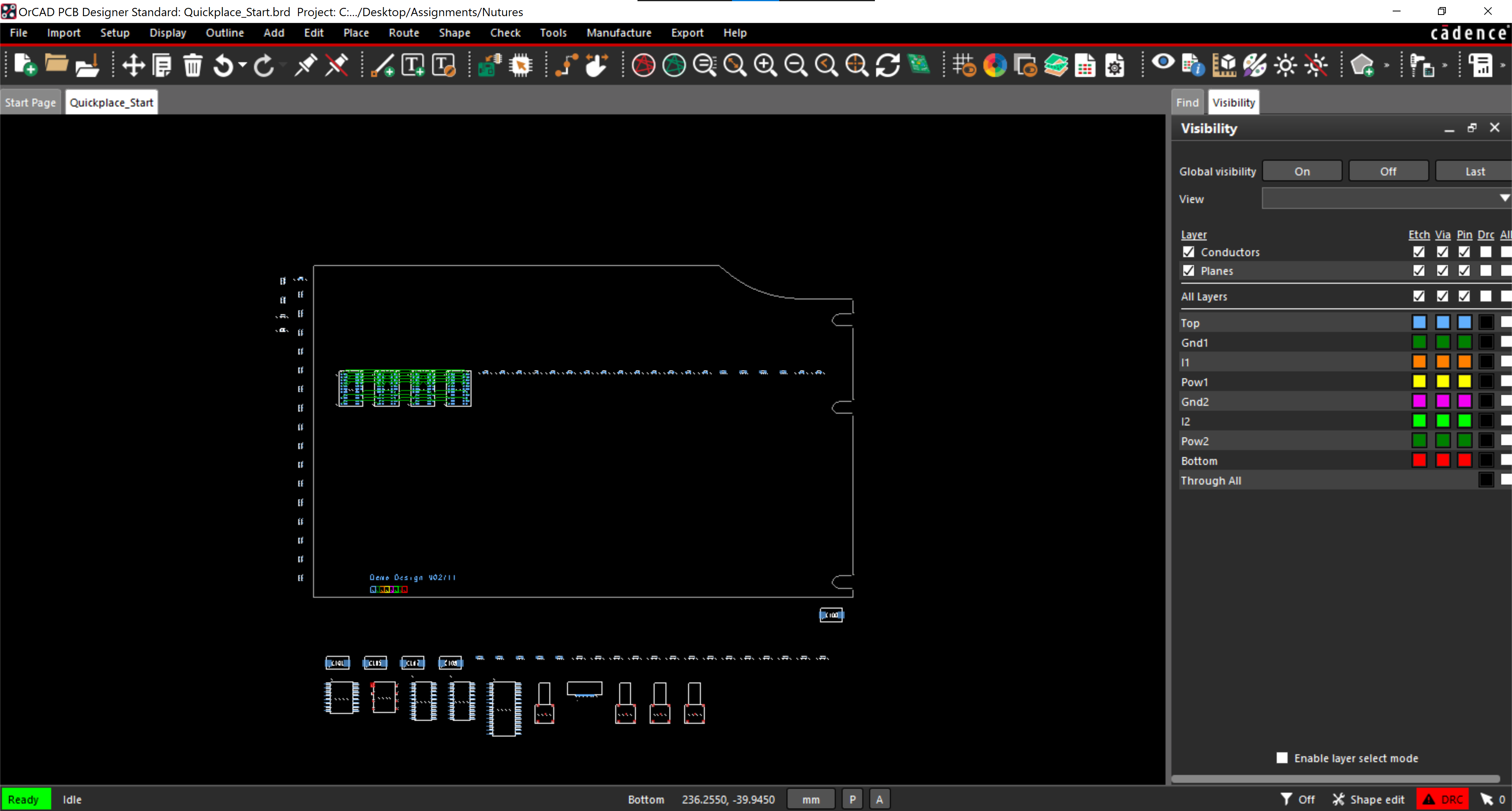
Component placement drives the entire PCB design. The ability to place components accurately and efficiently will save time and ensure success of your design. With customizable placement options using Quickplace in OrCAD, you can quickly and easily layout your board with placement by groups.
To follow along, you can download the design files here then, open the Quickplace_Start.brd in OrCAD PCB Designer Standard. Copy the symbols and padstacks in the Quickplace Footprints folder and paste the files into the standard PCB footprint library (C:CadenceSPB_17.4sharepcbpcb_libsymbols). View the completed placement with Quickplace_Finish.brd.
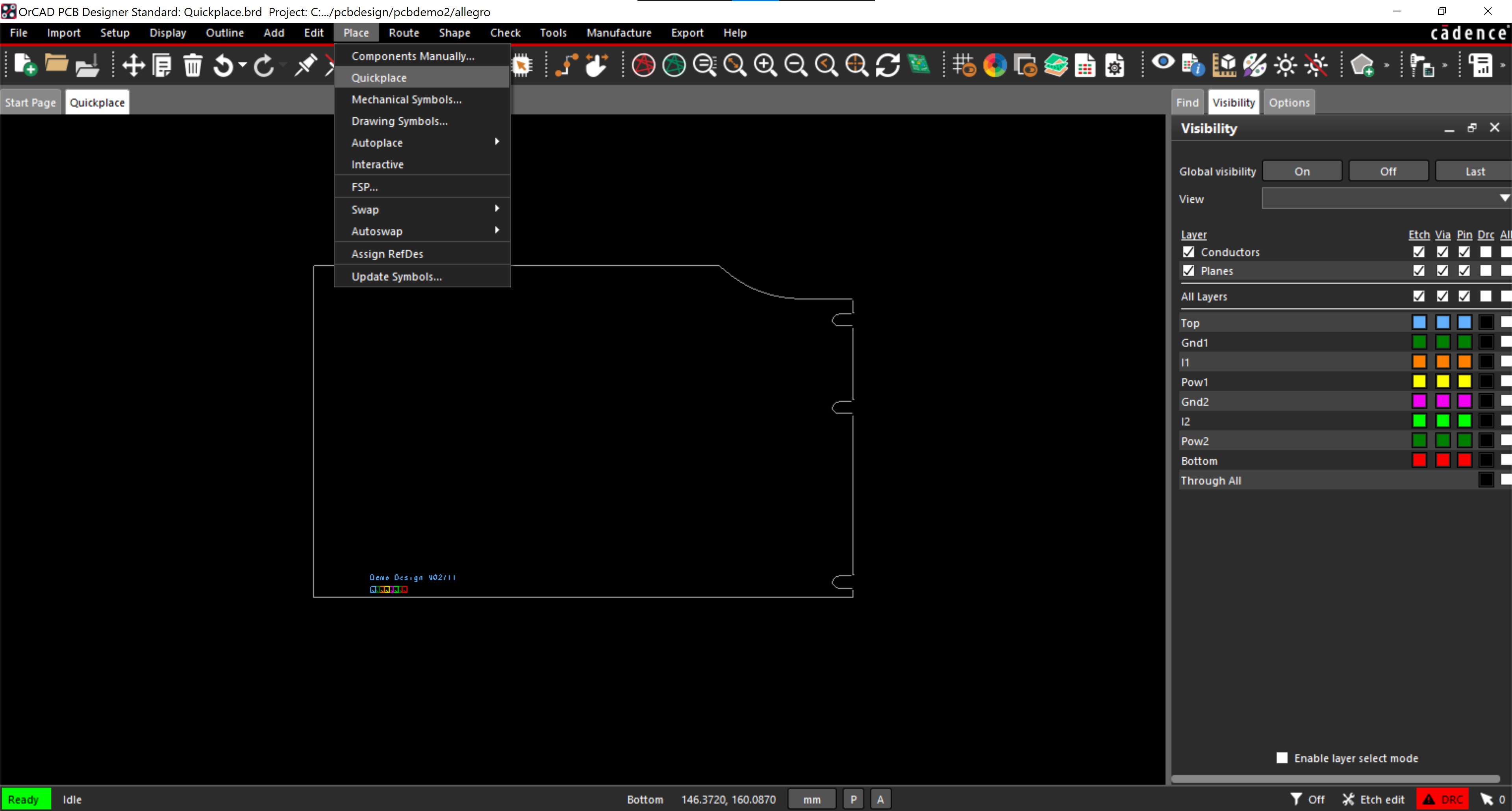
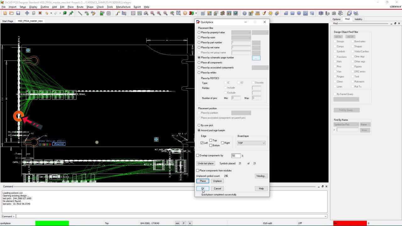
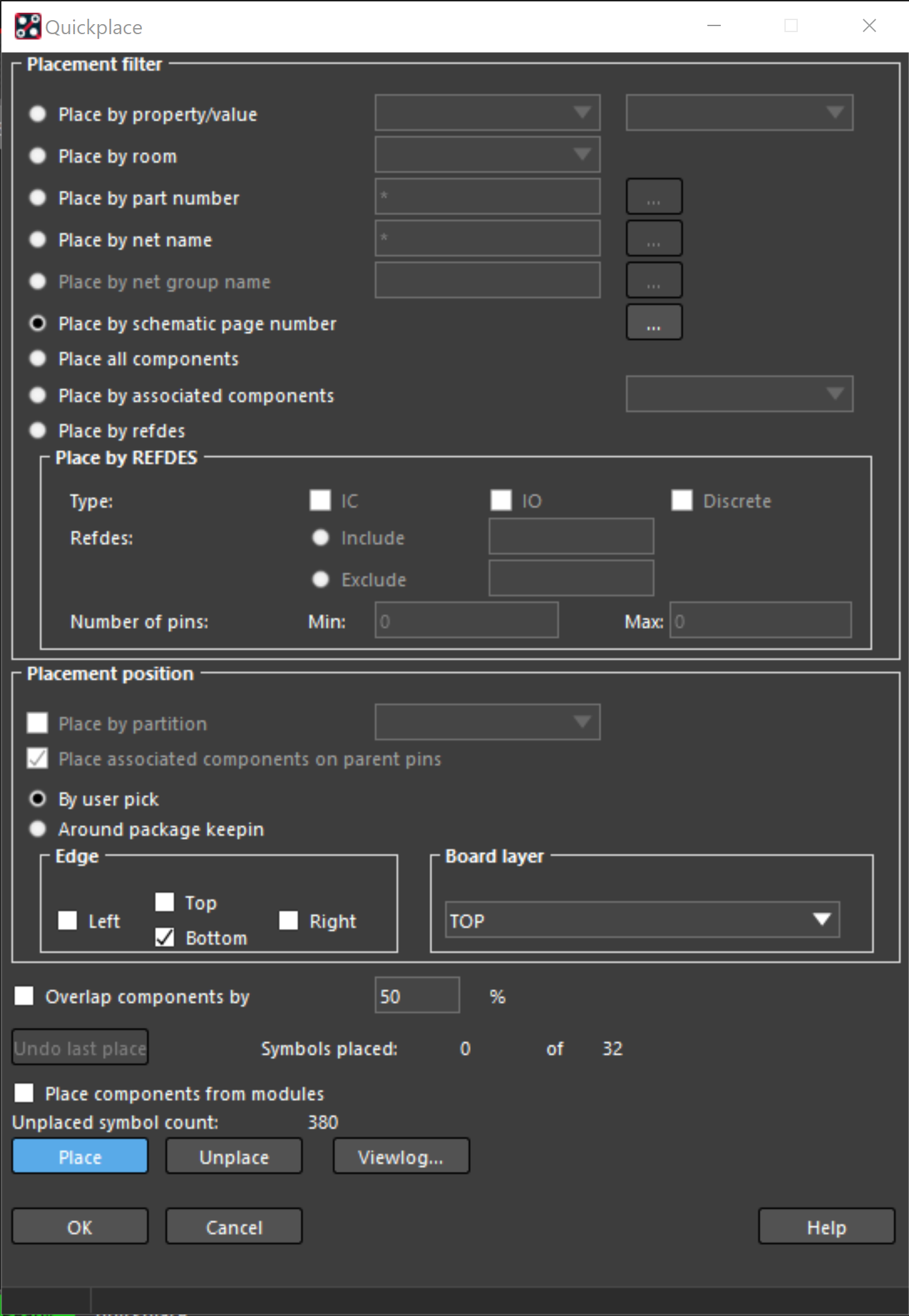
- Select Place > Quickplace from the menu.
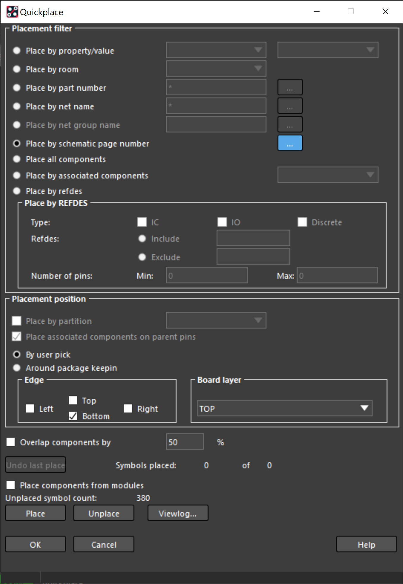
- Under Placement Position, select By user pick.
- Under Placement Filter, select Place by schematic page number.
- Click the Ellipsis to browse the schematic pages.
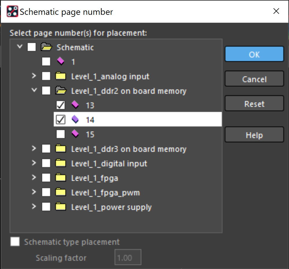
- Expand Level_1_ddr2 on board memory and select pages 13 and 14. Click OK.
- Select Place.
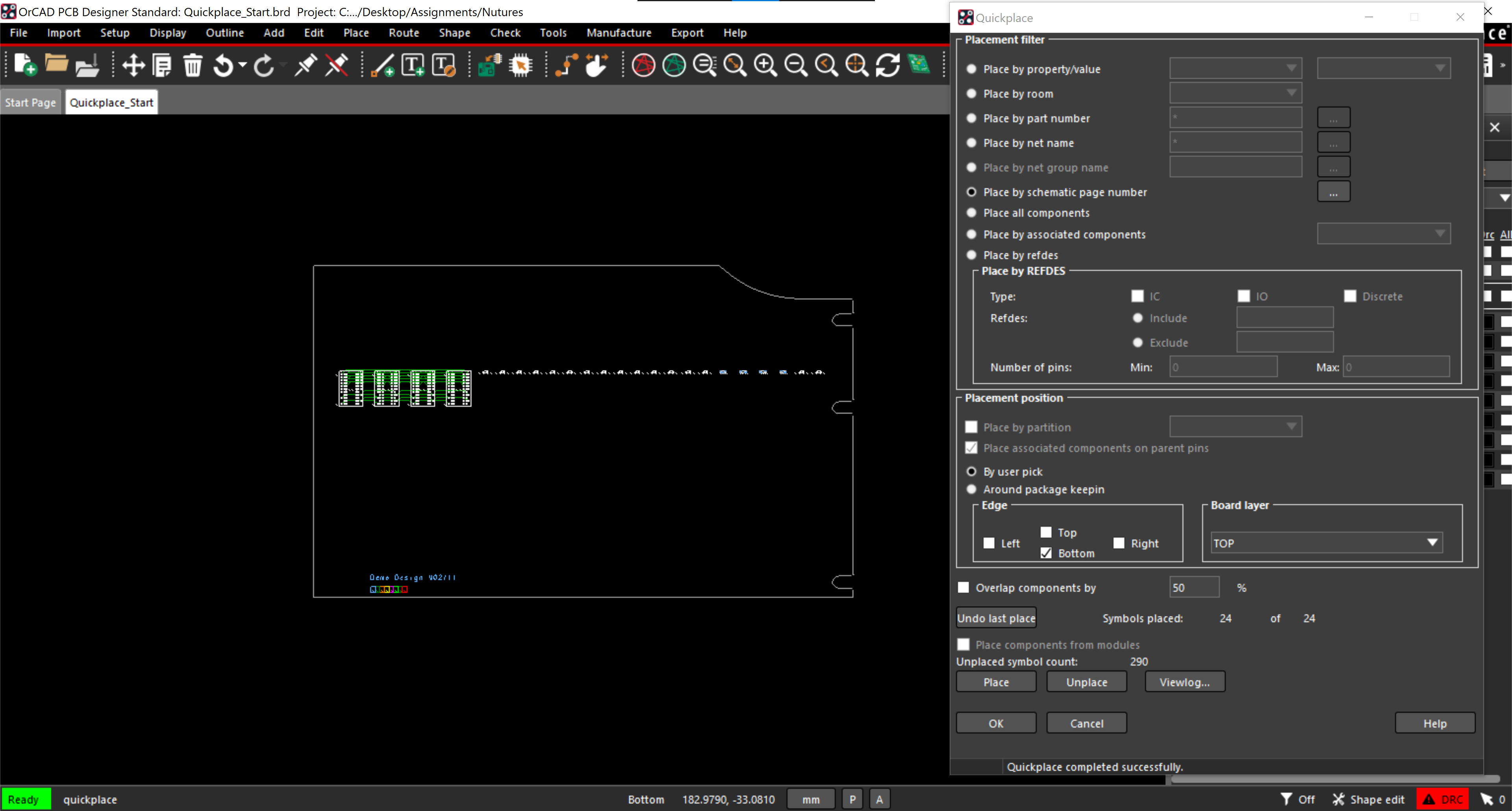
- Click the canvas to place the parts.

- In the Quickplace Window, select Around package keepin and Bottom under Placement position.
- Click the Ellipsis to browse the schematic pages.
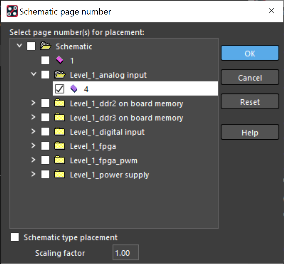
- Expand Level_1_analog input and select page 4. Click OK.
- Click Place.

- In the Quickplace Window, deselect Bottom and select Left under Placement position.
- Click the Ellipsis to browse the schematic pages.
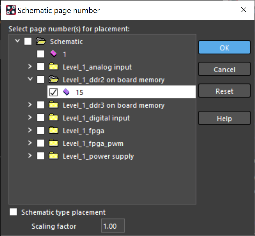
- Expand Level_1_ddr2 on board memory and select page 15. Click OK.
- Click Place.
- Click OK and close the Quickplace Window.
Save time laying out your PCB and focus on the design by placing components in groups with Quickplace in OrCAD PCB Designer.