The driving force behind technological advancements, like smarter consumer products and industrial Internet-of-things (IIoT), is the implementation of embedded systems. Introducing microprocessors transforms previously restricted capability devices and systems into computing environments. Doing so, enables unprecedented functionalities and necessitates understanding and incorporating additional data TX/RX schemes.
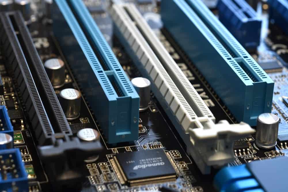
One of the major advantages of computing systems is the ability to communicate with various devices; such as peripherals, that add specialized functionalities to the system. Many of these devices, for example DDR memory modules, connect through Peripheral Component Interconnect Express (PCIe) slots. And designing PCBs that effectively utilize these interfaces and satisfy industry standard criteria requires incorporating essential PCI routing guidelines into your PCB layout best practices.
Essential PCIe Routing Guidelines
The best circuit board development processes signs seek to optimize all stages of the design⇒build⇒test or DBT cycle. For design, optimization is best achieved by implementing PCB design best practices; such as following your CM’s design for manufacturing and assembly (DFMA) rules and guidelines. It is equally important to tailor your PCB layout design to maximize signal and power transfer between board components and with connected elements; such as peripherals. Essential PCIe routing guidelines to consider to optimize your layout for data transfer with peripherals are listed below.
| ESSENTIAL PCIe ROUTING GUIDELINES | |
| PCIe Routing Guideline | Consideration |
| Route directional signals together | PCIe connectors consist of parallel pairs of unidirectional lanes. Routing TX signals on one layer and RX on the other is a good impedance matching technique for maximizing signal integrity. |
| Minimize via usage | Preferably, vias should not be used to route PCIe signals as the discontinuities promote noise and EMI. If unavoidable, minimize the number of vias and employ via shielding. |
| Follow spacing requirements | Just as for other trace routing, PCIe routes should adhere to industry standards for creepage and clearance distance spacing. |
| Ensure impedance matching for SMT fanouts | Ball-grid array (BGA) fanouts pose a challenge. It is important to maximize impedance matching between BGA pad and the via. Employing autorouting to create appropriately placed and sized via anti-pads is a good option. |
The considerations above are generically useful for PCIe routing designs. Depending upon your specific PCIe standard revision, EMI and impedance effects will vary. Therefore, it is important to adjust your board layout to accommodate the performance specifications and adhere to compliance standards for the PCIe version being implemented.
How to Best Achieve PCIe Compliance
Starting in 2003, standards were introduced by the Peripheral Component Interconnect Special Interest Group (PCI-SIG) to assist designers, developers and manufacturers in creating components and devices that would interconnect and operate efficiently. Adhering to the standard for a particular revision is deemed being PCIe compliant, which is essential to gain acceptance of your product and establish its marketability. Achieving PCIe compliance; however, is expensive and requires passing a set of rigorous tests. The best way to guard against testing failure(s), redesigns and excessive costs, is to design for compliance, as shown below.
Achieving PCIe Compliant PCB Design
- Know which performance metrics to test and range of acceptable values
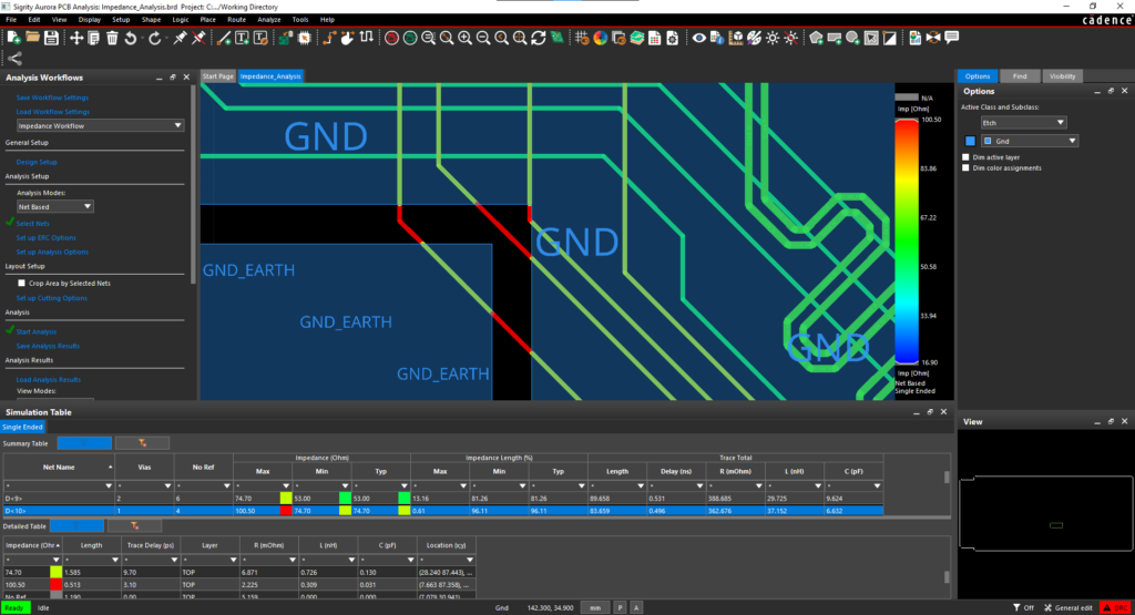
- Use simulation and analyze PCIe performance during PCB layout design
- Identify failures and potential non-compliance issues
- Follow PCIe routing guidelines when correcting non-compliance issues
See The Engineer’s Guide to PCIe for more details on how to ensure PCIe compliance during design.
As shown above, achieving PCB compliance is dependent upon following good PCIe routing guidelines. Whether you are new to PCB design or a seasoned veteran, it is best to employ PCB design and development software for the most effective design process and PCB development optimization.
EMA Design Automation is a leading provider of the resources that engineers rely on to accelerate innovation. We provide solutions that include PCB design and analysis packages, custom integration software, and engineering expertise, which enable you to create more efficiently. For more information on PCIe routing guidelines and how we can help you or your team innovate faster, contact us.


