|
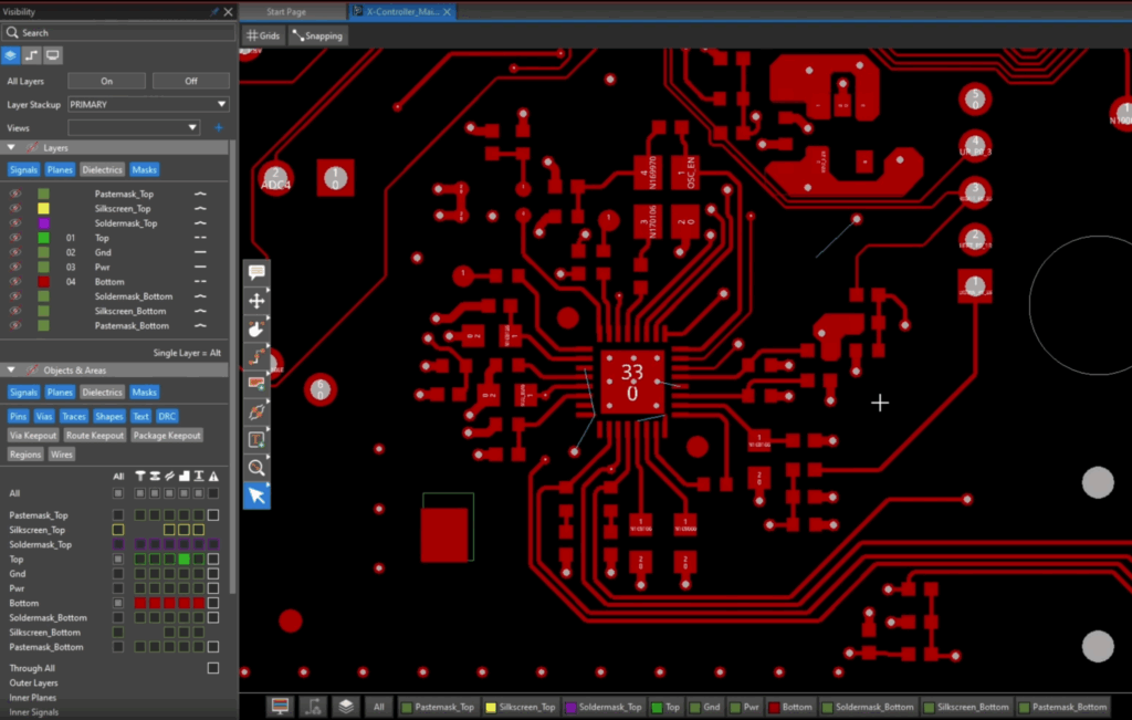
PCIe Gen 6: PCB Design Essentials |
|
|
Aspect |
Best Practice |
|
Signal Integrity |
✔ Use differential pairs with tight coupling to minimize noise and crosstalk. ✔ Maintain consistent trace impedance to match the characteristic impedance of PCIe Gen 6 (typically 85-100 ohms). ✔ Implement proper termination to avoid signal reflections. ✔ Use short and direct routing for high-speed signal paths to reduce latency and signal degradation. |
|
Power Integrity |
✔ Ensure a robust power delivery network (PDN) with low impedance across a wide frequency range. ✔ Use multiple ground planes to provide a stable reference and reduce electromagnetic interference (EMI). ✔ Implement decoupling capacitors close to the power pins of PCIe Gen 6 devices to filter high-frequency noise. |
|
Layer Stackup |
✔ Design a multilayer PCB with dedicated power, ground, and routing layers to improve signal integrity. ✔ Ensure proper layer spacing to control impedance and reduce EMI. |
|
Via Management |
✔ Minimize the use of vias in high-speed signal paths, as they can introduce impedance discontinuities. ✔ Use back drilling or blind/buried vias to reduce via stub lengths and improve signal integrity. |
|
Trace Length Matching |
✔ Ensure differential pair trace lengths are matched to minimize skew and ensure timing alignment. ✔ Keep trace lengths as short as possible to reduce propagation delay and signal loss. |
|
Routing Techniques |
✔ Avoid sharp bends in high-speed traces; use 45-degree angles or curved traces to reduce signal reflections. ✔ Route differential pairs together with equal length and spacing to maintain the differential impedance. |
|
Grounding |
✔ Implement a solid ground plane beneath high-speed signal traces to provide a low-inductance return path. ✔ Connect ground planes with vias to ensure a low-impedance path for return currents. |
|
Connector Placement |
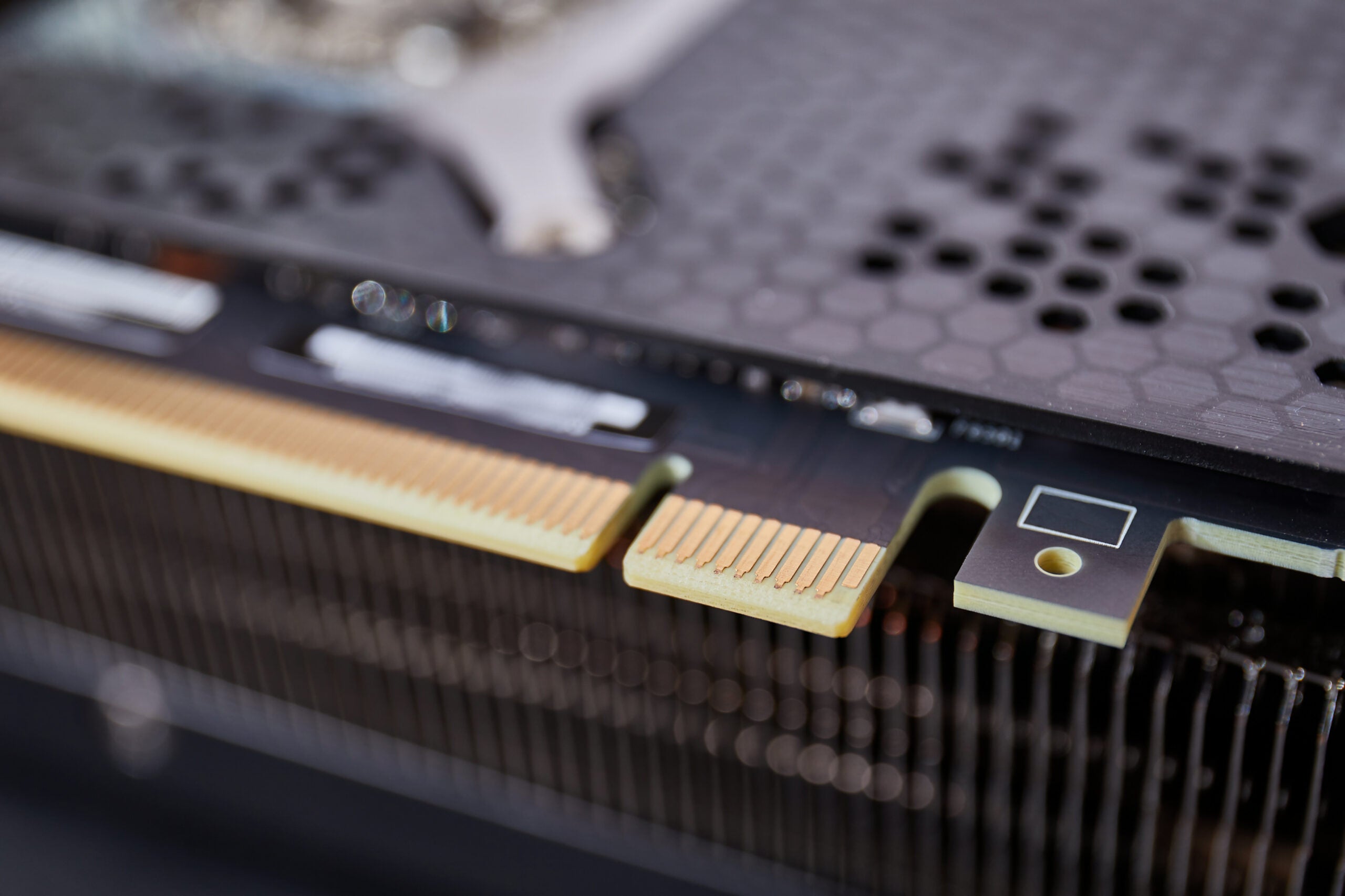
✔ Place PCIe Gen 6 connectors close to the board’s edge to reduce trace lengths and improve signal integrity. ✔ Ensure proper mechanical support for connectors to maintain signal integrity under mechanical stress. |
|
Thermal Management |
✔ Implement adequate cooling solutions (e.g., heatsinks, fans) to manage heat dissipation from high-speed PCIe Gen 6 devices. ✔ Use thermal vias and copper pours to enhance heat dissipation through the PCB. |
|
Simulation and Testing |
✔ Perform signal integrity simulations to validate the design before fabrication. ✔ Conduct pre-layout and post-layout simulations to identify and mitigate potential issues. ✔ Perform thorough testing and validation of the PCB to ensure compliance with PCIe Gen 6 specifications. |
PCIe Gen 6 Features and Applications
PCIe Gen 6 doubles the data transfer rate and lane speed of PCIe Gen 5, while introducing error correction for enhanced reliability at these higher speeds. Both versions remain backward compatible with previous generations. To better understand the features enabled by PCIe Gen 6, let’s compare them to PCIe Gen 5.|
PCIe Gen 5 vs PCIe Gen 6 |
||
|
Feature |
PCIe 5.0 |
PCIe 6.0 |
|
Data Rate |
32 gigatransfers per second (GT/s) per lane |
64 GT/s per lane |
|
Maximum Bandwidth |
128 gigabytes per second (GB/s) (x16 configuration, bidirectional) |
256 GB/s (x16 configuration, bidirectional) |
|
Encoding Scheme |
NRZ (non-return-to-zero) |
PAM-4 (pulse amplitude modulation with 4 levels) |
|
Forward Error Correction (FEC) |
No |
Yes, low-latency FEC |
|
Flow Control Unit (Flit) Mode |
No |
Yes, new flit-based encoding |
|
Latency |
Low |
Lower due to improved protocols and FEC |
|
Power Efficiency |
Improved over previous generations |
Further improved efficiency |
|
Backward Compatibility |
Compatible with PCIe 4.0, 3.0, 2.0, and 1.0 |
Compatible with PCIe 5.0, 4.0, 3.0, 2.0, and 1.0 |
|
Channel Reach |
Similar to PCIe 4.0 |
Improved equalization techniques for longer reach |
|
Signal Integrity Requirements |
High |
Higher due to increased data rates |
- Data Centers: Increased data transfer speeds and efficiency make PCIe Gen 6 ideal for data center applications, where fast and reliable data access is crucial.
- AI and Machine Learning: PCIe Gen 6’s high bandwidth and low latency support the demanding data requirements of AI and machine learning workloads.
- High-Performance Computing: PCIe Gen 6’s enhanced performance benefits high-performance computing applications, such as scientific simulations, financial modeling, and other data-intensive tasks.
- Networking: PCIe Gen 6 improves the performance of network interface cards (NICs) and other networking equipment, supporting faster and more efficient data transmission.


