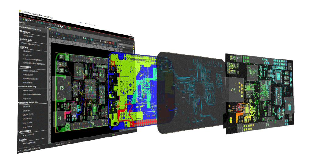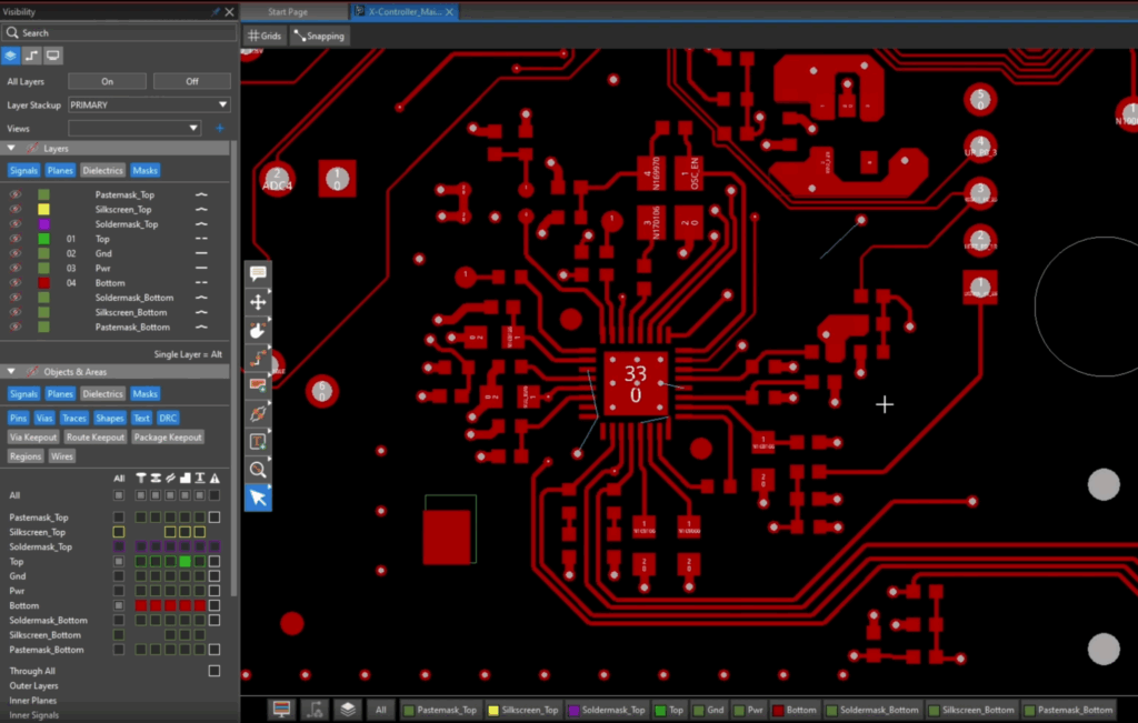
A PCB stackup design is the arrangement of repeating conductive and insulating layers within a PCB most often to accommodate signal flow through vias. The stackup determines how signals are routed and how the board handles power distribution and electromagnetic interference (EMI) on and between layers. Especially important for high-speed boards, is the following of important PCB stackup design guidelines. Doing so enables designers to effectively manage signal integrity issues, reduce crosstalk, and ensure board functionality.
Important Guidelines for PCB Stackup Design
Designing your board’s stackup requires the consideration of several factors, as listed below.
PCB STACKUP DESIGN CONSIDERATIONS AND GUIDELINES | |
PCB Stackup Design Factors | Guidelines |
Controlled Impedance | – Select appropriate dielectric materials, trace widths, and separation distances for controlled impedance. – For precise control, use a field solver over general equations. – Place signal layers near reference ground planes; avoid routing high-speed signals on outer layers unless necessary. |
Interplane Capacitance | – Place power and ground planes within 3 mils or closer to achieve interplane capacitance, reducing high-frequency noise. – Select high dielectric constant (DK) materials to increase capacitance between planes. – Useful in high-speed applications to minimize external decoupling capacitors and enhance power integrity. |
Lamination Type | – Standard FR4 is suitable for common boards, while high-performance laminates like FR408HR or Rogers 4000 are better for high-speed or high-frequency applications. – Foil lamination: Cost-effective and simple, ideal for most PCBs. – CAP lamination: Preferred for rigid, high-frequency designs or materials like Rogers 4350. – Sequential lamination: Recommended for HDI or advanced RF designs with blind and buried vias, though costly. |
| Prepreg and Laminate Selection | – Use thin prepregs and laminates between signal and reference layers for optimal impedance and minimal signal degradation. – Low DK materials are preferred for high-speed signal layers to control impedance variation. – Thicker laminates and multiple prepregs stabilize power planes and reduce thermal expansion risks. – Thinner prepregs on signal planes ensure tight coupling with reference planes for controlled impedance. |
Material Selection | – Choose materials with stable dielectric constants and low loss tangents, especially important for high-speed applications. – Ensure material availability to avoid supply chain delays and ensure consistency across manufacturing. |
| Signal Layer Positioning | – Adjacent signal layers to a ground or power plane provide a stable return path, reducing inductive noise. – Ensures return paths are consistent, minimizing reflection and noise issues across both analog and digital signals. |
Ground Plane Configuration | – Continuous ground planes reduce ground impedance, enabling stable current distribution for high-frequency designs. – Uninterrupted ground planes connected to power layers enhance signal grounding. – Supports microstrip or stripline configurations, minimizing interference from nearby signal paths or external sources. |
| Power and Ground Plane Coupling | – Tight coupling of power and ground planes results in low impedance and reduced signal interference, benefiting EMC. – Close plane spacing improves decoupling capacitance and stabilizes power delivery to components. – Acts as a shield, reducing external noise and protecting sensitive components from internal noise. |
Signal Layer Insulation | – Thinner insulation between signal and adjacent planes enhances capacitive coupling, reducing EMI and crosstalk in high-speed designs. – Minimal insulation thickness allows for controlled impedance, essential for signal integrity in RF/high-frequency applications. – Ensures stable signal return paths and reduces inductive interference across the PCB stackup. |
| Sequential Layer Arrangement | – Arrange layers to maximize signal integrity and thermal performance by placing signal layers between ground/power planes. – Avoid placing two signal layers adjacent to prevent noise issues and coupling between signals. – Symmetric arrangements (e.g., mirroring top/bottom layers inward) reduce warping and improve mechanical stability. – Use microstrip configurations with minimal dielectric thickness between signal and reference planes for high-speed routing, reducing signal loss and latency. |
Sequential Lamination | – Limit lamination steps to control manufacturing costs; sequential lamination allows staged addition of layers for blind/buried vias. – Each step increases complexity and cost; consult manufacturers for material compatibility with sequential lamination. – Avoid excessive copper to prevent heat buildup during lamination. – Limit sequential laminations to three stages or fewer for cost efficiency, ensuring alignment and adhesion stability. |
Common PCB Stackup Layer Configurations
Although circuit boards can be built to include dozens of layers, generally, stackups come in even numbers (e.g., 2-layer, 4-layer, 6-layer, and 8-layer). 2-layer configurations are used for the simplest designs or where minimal restriction on board routing real estate exists. However, demand for smaller devices and systems makes higher layer counts more typical for many applications.
PCB Stackup Design for 4-Layer Boards
Four-layer PCBs are often used in applications with moderate complexity and performance. A typical stackup for a 4-layer board includes two signal layers and two plane layers for ground and power.
- Top Layer (Signal 1): High-speed signals and components.
- Inner Layer 1 (Ground Plane): Continuous ground plane for signal return paths.
- Inner Layer 2 (Power Plane): Dedicated power plane to distribute power uniformly.
- Bottom Layer (Signal 2): Additional routing for signals
PCB Stackup Design for 6-Layer Boards
A 6-layer PCB offers more flexibility for routing and better control over signal integrity, making it more appropriate for high-speed applications.
- Top Layer (Signal 1): Critical high-speed signals.
- Inner Layer 1 (Ground Plane): Solid ground plane.
- Inner Layer 2 (Signal 2): High-speed differential pairs.
- Inner Layer 3 (Signal 3): General routing for less critical signals.
- Inner Layer 4 (Power Plane): Dedicated power plane.
- Bottom Layer (Signal 4): Additional signal routing.
4 and 6-layer stackups are often used in similar systems and share PCB stackup design considerations, as shown below.
4 TO 6-LAYER PCB STACKUP DESIGN CONSIDERATIONS | ||
Criteria | 4-Layer Stackup | 6-Layer Stackup |
Impedance Control | Requires controlled impedance paths for high-speed signals, typically achieved by placing a ground plane next to signal layers. | Provides better impedance control by enabling routing of critical signals between ground planes, reducing noise and crosstalk. |
Noise Reduction and Signal Integrity | Limited noise reduction capabilities due to a single ground plane, offering minimal shielding for high-speed signals. | Additional ground planes improve EMI control and provide effective shielding for high-speed signals, making it suitable for designs with strict noise requirements. |
Power Delivery and Thermal Management | Includes a power plane but offers basic power distribution and thermal management. | Enhanced power delivery due to additional layers, allowing more stable current distribution and improved thermal dissipation, beneficial for high-power applications. |
| Routing Strategy | Limited routing space requires careful management of high-speed signals near the ground plane to avoid impedance mismatches. | Increased routing flexibility with inner layers, allowing easier management of critical signal paths and differential pairs, enhancing signal integrity and reducing interference. |
Applications | Suitable for basic electronic devices, low-frequency analog circuits, and low- to medium-speed digital circuits with moderate EMI control requirements. | Ideal for high-speed digital applications and RF circuits where enhanced EMI control and signal integrity are essential. |
PCB Stackup Guidelines for 8-Layer Boards
For even more complex designs, such as those involving high-speed data transmission and dense component placement, an 8-layer PCB stackup is ideal. This stackup provides increased flexibility for routing and superior control over EMI and impedance.
- Layer Arrangement: a typical arrangement is Signal 1 (top), Ground, Signal 2, Power, Signal 3, Ground, Signal 4, and Signal 5 (bottom). The increased number of layers allows designers to separate power and ground planes, dedicating entire layers to routing critical high-speed signals, increasing signal integrity.
- EMI Control and Shielding: The additional ground planes in an 8-layer stackup offer superior EMI control by “sandwiching” high-speed signals between ground planes, creating isolated paths.
- Improved Power Distribution: The 8-layer stackup has multiple dedicated power and ground planes, which stabilize current distribution and minimize voltage fluctuations —particularly useful in high-power applications. Additionally, the layered structure improves thermal dissipation, enabling the PCB to handle higher power levels.
- Precise Layer Separation for Controlled Impedance: An 8-layer PCB allows designers to control the separation between signal and ground planes.
- Applications: 8-layer PCBs are commonly deployed in high-speed computing devices, telecommunications equipment, and RF systems where signal integrity, low EMI, and efficient heat dissipation are crucial, i.e., boards with dense routing and high-frequency signal transmission.
Today’s compact circuit board designs necessitate that essential PCB stackup design issues be understood and guidelines followed. This is essential for rigid and rigid-flex stackups to ensure functionality and performance objectives are met, while adhering to dimensional and installation constraints.
EMA Design Automation is a leading provider of the resources that engineers rely on to accelerate innovation. We provide solutions that include PCB design and analysis packages, custom integration software, engineering expertise, and a comprehensive academy of learning and training materials, which enable you to create more efficiently. For more information on HDI PCB design guidelines and how we can help you or your team innovate faster, contact us.


