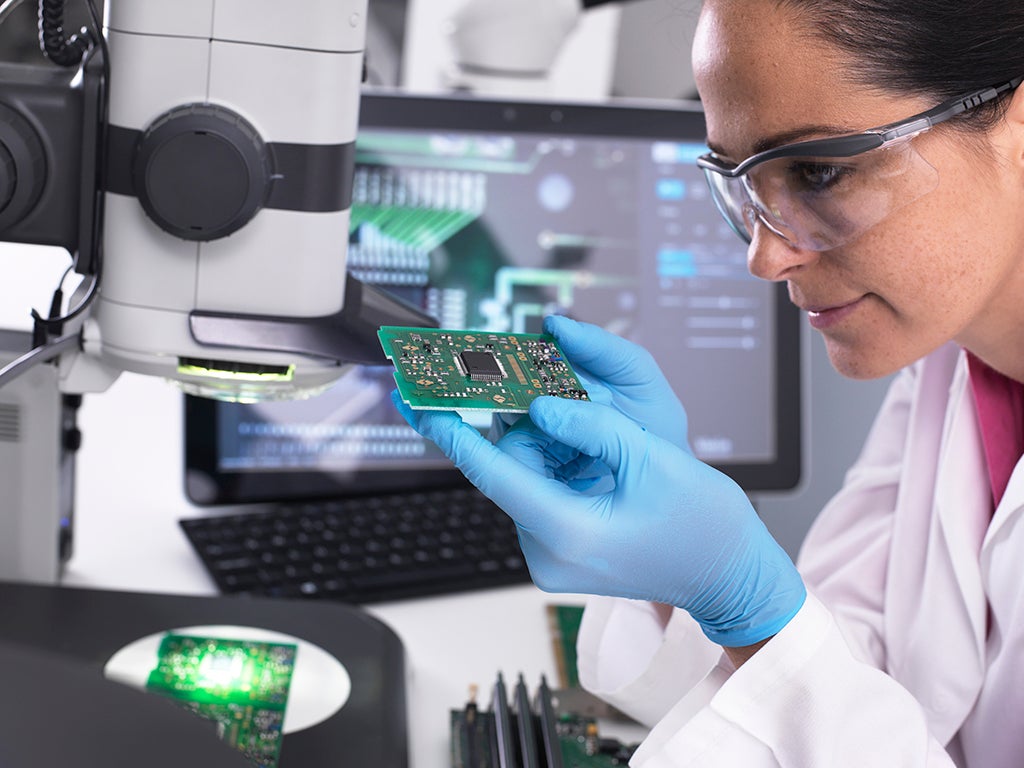
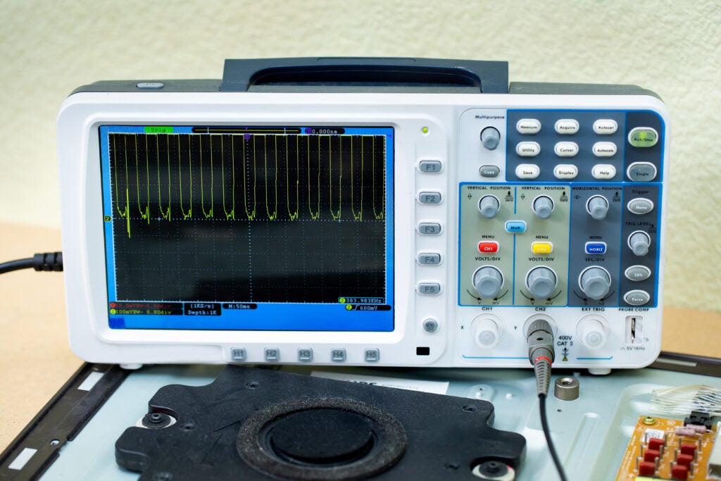
 PCB simulation tools enable engineers to identify and resolve potential problems before boards are produced, thereby reducing costly errors and rework. Using these tools, engineers can test for signal integrity, power integrity, thermal performance, electromagnetic compatibility, and other metrics. Simulation tools streamline development, lower costs, and accelerate time to market by ensuring high-quality, functional, and manufacturing-ready designs. Below is a list of the most essential PCB simulation tools engineers should have.
|
PCB Simulation Tools |
||
|
Simulation Area |
Tools |
Importance |
|
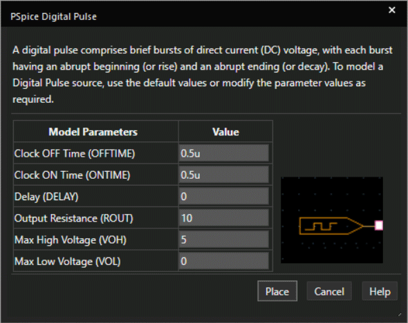
SPICE Simulation |
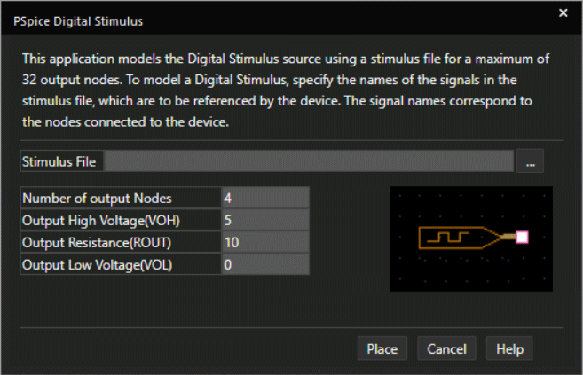
PSpice, LTspice, ngspice |
Performs circuit simulation to validate electrical performance before layout. |
|
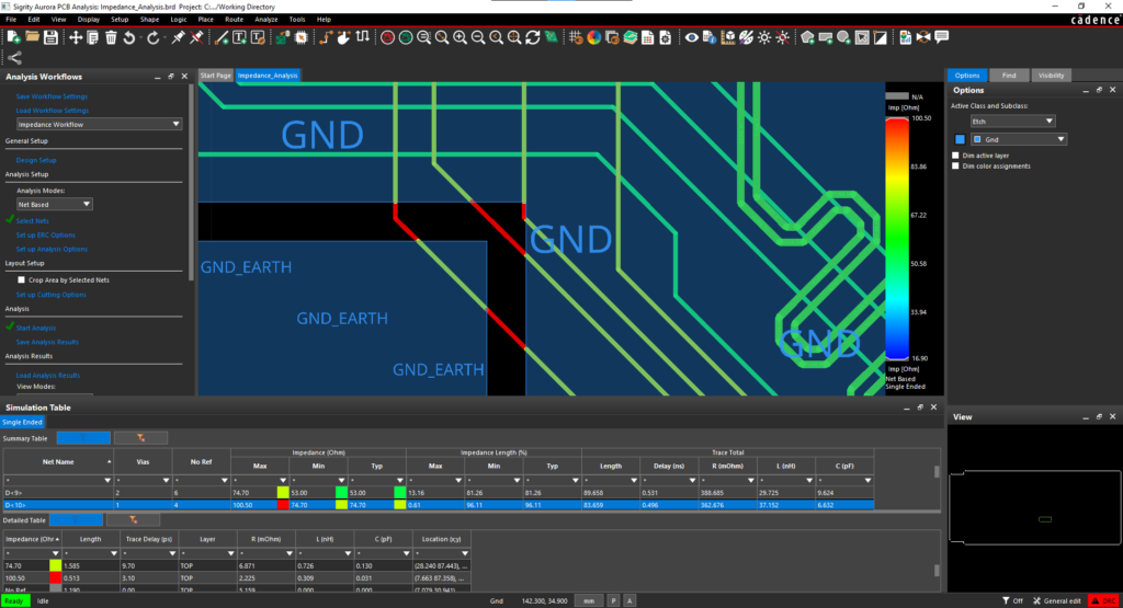
Signal Integrity (SI) Analysis |
Sigrity, HyperLynx, SIwave |
Analyzes high-speed signal behavior to prevent reflection, distortion, crosstalk and noise. |
|
Power Integrity (PI) Analysis |
Sigrity, SIwave, PowerDC |
Ensures stable power delivery, reducing voltage drops and power noise issues. |
|
Celsius Studio, Pollex, SOLIDWORKS, Simcenter Flotherm, COMSOL Multiphysics |
Predicts heat distribution and prevents overheating, ensuring thermal reliability. |
|
|
Electromagnetic Compatibility/Electromagnetic Interference (EMC/EMI) |
Sigrity, Simulia, EMC Plus |
Detects and mitigates EMC/EMI to improve circuit performance and meet regulatory compliance. |
|
Topology Extraction |
Sigrity, OrCAD X, Altium, HyperLynx |
Provides a means of “reverse engineering” board layout prior to manufacturing to enable schematic model simulations. |
|
High-Speed Design Validation |
AWR, CST Studio, PathWave, Xpedition |
Supports complex, high-frequency PCB designs by optimizing signal routing. |
|
3D Mechanical Fit & PCB Layout |
MCAD X, Fusion 360, Altium 3D Viewer, SOLIDWORKS |
Ensures efficient ECAD-MCAD integration and prevents assembly issues. |
|
Manufacturing Design Verification |
OrCAD X, Valor NPI, CAM350 |
Checks manufacturability constraints and DFM issues to avoid fabrication defects. |
Benefits of Using PCB Simulation Tools
PCB simulation tools are a great way to test circuit boards before physical prototyping. The key benefits of these tools include:1. Cost Savings
- Saves money by lessening the need for physical prototypes.
- Reduces the need for expensive reworking or design failures by flagging errors early.
2. Time Efficiency
- Accelerates PCB design by finding issues before manufacturing.
- Enables fast iterations and optimizations, reducing development cycles.
3. Error Detection and Debugging
- Identifies design flaws such as signal integrity, power distribution, and thermal issues.
- Simulates electrical behavior to ensure functionality.
4. Performance Optimization
- Enables designers to test and fine-tune circuit behavior under various conditions.
- Optimizes trace routing, power consumption, and signal integrity.
5. Reliability Improvement
- Allows for stress testing for voltage, current, and thermal effects to improve durability.
- Prevents design failures from environmental factors or operational stress.
6. Enhanced Collaboration
- Enables sharing of simulations and results with teams globally.
- Integrates with CAD tools for a seamless workflow.
7. Compliance Verification
- Verifies that PCB designs meet industry standards.
- Mitigates regulatory compliance issues before production.
8. 3D Visualization and Analysis
- Provides a virtual representation of the PCB to check clearances, mechanical fit, and component placement.
- Reduces mechanical design problems before assembly.
9. Improved Decision-Making
- Enables comparisons of design choices without physical testing.
- Aids in selecting the best materials, components, and layout strategies.
10. Integration with Manufacturing Processes
- Ensures the design is optimized for manufacturability and testability.
- Lessens production errors and improves yield rates.
EMA Design Automation is a leading provider of the resources that engineers rely on to accelerate innovation. We provide solutions that include PCB design and analysis packages, custom integration software, engineering expertise, and a comprehensive academy of learning and training materials, which enable you to create more efficiently. For more information on integrating PCB simulation tools into your design workflow and how we can help you or your team innovate faster, contact us.


