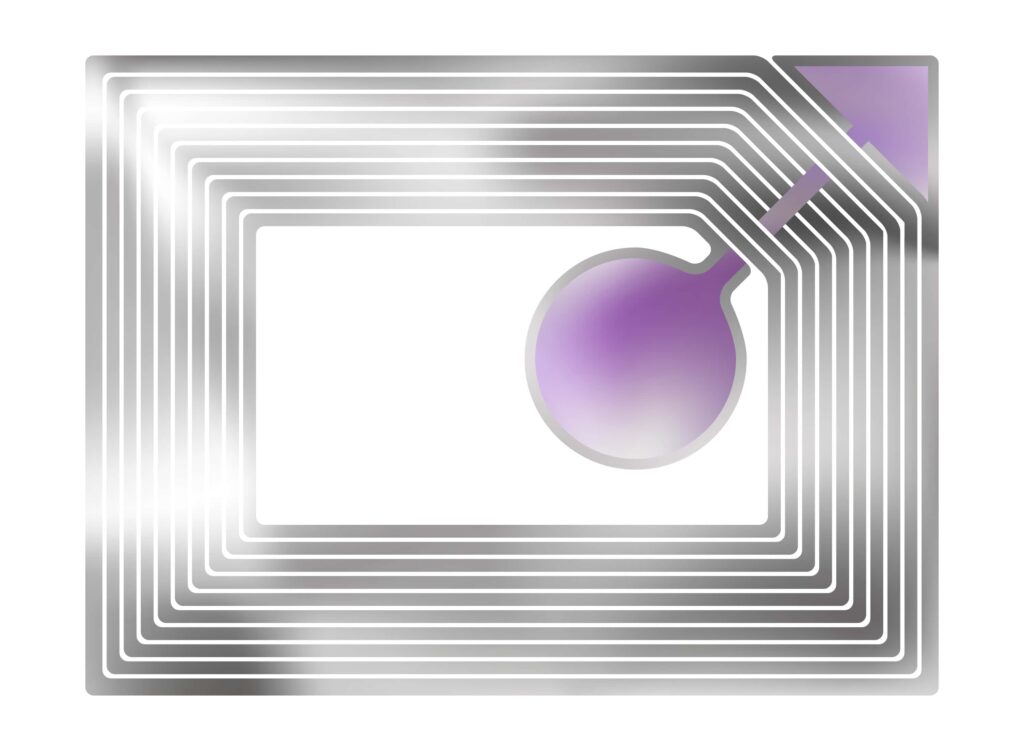
As the use of wireless data and energy transmission proliferates so does the need for PCB antennas. For many applications, the use of externally connected, often bulky antennas, is impractical or too costly. For these cases, engineers turn to monopoles, dipoles, patch or loop antennas.
Loop antennas, in particular, are typically employed as receivers in applications; such as radio-frequency identification (RFID) technology systems. Although relatively simple in operation, these devices are quite versatile. By understanding implementation options and following PCB loop antenna design best practices, you can optimize performance and reliability.
PCB Loop Antenna: Pros and Cons
PCB LOOP ANTENNA DESIGN | |
Advantages | Disadvantages |
Simplicity | Inefficient transmission |
Versatility | Low radiation resistance |
Low cost | Not usable at high frequencies |
As shown in the table above, there are important limitations that restrict the use of PCB loop antennas. For example, loops are relatively poor for long range signal transmission and are best used at low to mid frequencies. Yet, their simple construction, flexibility in terms of size and shape and low cost make these antennas preferable for near field wireless applications like RFID tag readers and cellular phone chargers.
Types of Loop Antennas
PCB loop antenna designs may be circular, elliptical, triangular, square or rectangular in shape. Sizes vary as well; however, for PCB implementation compactness is a major positive attribute. Typically, loop antennas are classified as small, medium, or large:
Small loop antenna is also known as a magnetic loop. These antennas exhibit symmetrical electrical characteristics and are minimally susceptible to interference or noise.
Medium loop antenna exhibits directional radiation patterns or polarization based on the point of feed into the loop. For full-wavelength axial mounting, power distribution is even throughout the loop.
Large loop antenna is essentially a dipole antenna. These antennas are capable of higher energy transfer, as compared to the other types.
Loop antennas are similar to other radiating elements in that maximum power transfer occurs when a good impedance matching technique is employed.
Optimizing Your PCB Loop Antenna Design
PCB loop antenna designs are often implemented as sub-circuits connected via coaxial or another connector type. However, smaller loops–due to their good EMI and EMC attributes–can be included on a single PCB with other components. In either case, incorporating good PCB layout design guidelines is essential to achieve the best results. For example, it is critical to follow creepage and clearance standards when your design includes radiators, like loop antennas.
Guidelines for PCB Loop Antenna Design Optimization
- Prioritize antenna impedance matching network design to minimize losses and maximize RX/TX power transfer.
- Use clearance and creepage distance tables to maximize signal propagation and minimize interference based on voltage and frequency levels.
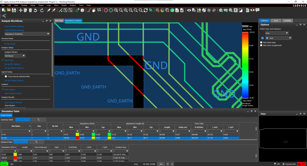
- Employ a simulation tool to analyze and verify signal integrity (SI) and power integrity (PI) performance.
- Utilize effective PCB layout design software.
As shown above, there are important considerations and design steps that should be employed when designing loop antenna circuit boards. For more direction on best practices for PCB loop antenna design, see “How to Design Spiral Inductors on a PCB.”
EMA Design Automation is a leading provider of the resources that engineers rely on to accelerate innovation. We provide solutions that include PCB design and analysis packages, custom integration software, engineering expertise, and a comprehensive academy of learning and training materials, which enable you to create more efficiently. For more information on best practices for PCB loop antenna design and how we can help you or your team innovate faster, contact us.


