PCB layout efficiency is essential for a designer’s workflow. Using advanced CAD tools and good design techniques, key aspects such as component placement, signal flow, power distribution, and thermal considerations, can be optimized for better functionality and manufacturability. Read on as we discuss these aspects, as well as recent advancements in OrCAD X 24.1, that further aids in increased efficiency.
TOOLS AND METHODS FOR PCB LAYOUT EFFICIENCY | |
PCB Layout Aspects | Tools/Methods |
Footprint Creation | – Common Package Types: Leverage common component package types to streamline processes and minimize errors. – Accurate CAD Models: Ensure component CAD models are based on datasheets or other verifiable manufacturer part information. – Customization: The ability to customize pin numbers and spacing, whether from scratch or for standard packages, is important. – 3D Formats: CAD models that include 2D and 3D rendering and dimension specification is important to facilitate efficient ECAD-MCAD integration. |
Component Placement | – Functional Grouping: Place components logically by grouping them according to their functions. This reduces trace lengths and simplifies routing. – Proximity Considerations: Place high-speed components close to connectors or other critical components to reduce signal delays and potential interference. – Design for Manufacturability (DFM): Ensure that components are placed with sufficient spacing to meet manufacturing tolerances and facilitate assembly. – Consider Mechanical Constraints: Account for board edges, mounting holes, and mechanical enclosures to prevent conflicts in the final product. – Use Placement Constraints: Define placement constraints in your design software to automatically enforce rules for component spacing and orientation. |
Signal Flow | – Direct Routing Paths: Keep traces as short and direct as possible to minimize inductance and resistance, which can degrade signal quality. – Controlled Impedance Routing: Use impedance-controlled traces for high-speed signals to prevent signal reflections and losses. – Differential Pair Routing: Employ differential pairs for signals that require high noise immunity, ensuring the pair is routed together with consistent spacing. – Layer Management: Dedicate specific layers to signal routing, power planes, and ground planes to reduce crosstalk and EMI. – Via Minimization: Reduce the number of vias in critical signal paths to prevent impedance discontinuities and signal degradation. – Proper Termination: Implement appropriate termination resistors to match the characteristic impedance of transmission lines. – Use Signal Integrity Analysis Tools: Employ simulation and analysis tools (available in OrCAD X) to predict and mitigate signal integrity issues before manufacturing. |
| Power Distribution | – Star Routing: Implement star topology for power distribution to ensure each component receives a clean power supply without interference from others. – Thermal Vias: Incorporate thermal vias in power pads to dissipate heat and enhance current-carrying capabilities. – Voltage Drop Analysis: Use simulation tools to analyze voltage drops across the PDN and adjust the design accordingly. |
Accurate PCB Footprints: The Foundation for PCB Layouts
Component footprints are the foundation of PCB layout design and best practice guidelines should be followed to ensure that accurate footprints are created. Doing so is critical for the veracity of trace routing and to avoid board build problems. Manufacturability issues caused by footprint dimensional inaccuracy include: failed pick and place, solder bridging due to component-pad misalignment, and other contingencies that will require redesign and respin.
The new OrCAD X release includes a footprint wizard that significantly simplifies the process. For example, common industry packages and predefined footprints are easily retrievable and modifiable to meet your layout design requirements and 3D models are automatically generated from footprint parameters. The integrated Layout Editor delivers advanced functionality for more complex component footprint creation needs.
PCB Layout Efficiency Through Component Placement
Properly positioning components reduces signal interference, minimizes trace lengths, and facilitates easier routing. To optimize component placement, designers should focus on functional grouping, maintaining a logical signal flow, and considering mechanical constraints like board edges and mounting holes. Utilizing grid systems for alignment and enforcing design-for-manufacturability (DFM) rules also aids in determining where your components are able to be placed. Effective placement should minimize trace lengths and reduce routing complexity while ensuring proximity to critical components, like connectors.
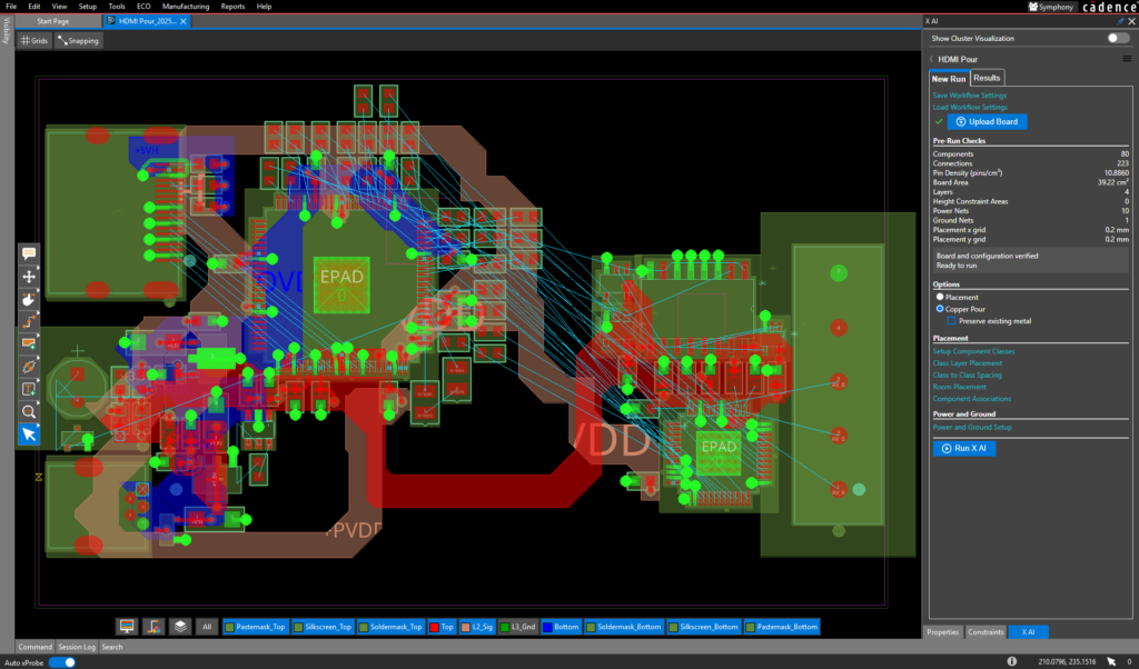
OrCAD X 24.1 introduces an enhanced Move command that significantly improves the component placement process. With features like dynamic heads-up display (HUD), alignment guides, and the ability to move components using keyboard shortcuts, designers can position components more precisely and efficiently. The command also supports rip-up or slide etch, making it easier to adjust placements without extensive rework. Additionally, OrCAD X 24.1 includes new functionality to enhance grouping of components such as automatic component placement according to the logical layout in the schematic. This will replicate the placement of components on the PCB to keep connections short while placing components in functional groups.
Signal Flow Management for PCB Efficiency
In optimizing PCB layout efficiency for signal flow, maintain consistent trace widths, and apply a proper termination for high-speed signals. Employing tools that control impedance for high-speed signals, and differential pair routing for noise-sensitive traces can also result in a more efficient layout. Minimizing vias, and ensuring proper termination is important, especially for high frequency signals. Utilizing software tools that enable signal integrity analysis and impedance matching is invaluable for optimizing high-frequency designs.
The latest version of OrCAD X enhances signal flow optimization with improved routing capabilities. The Scalpel tool allows designers to slice through existing routes, simplifying the process of editing and reusing circuitry. Features like Ultra Shadow mode and customizable net coloring make it easier to navigate complex nets, ensuring that signal paths are clear and well-organized. OrCAD X also aids in impedance control within the Cross Section Editor. Designers can set layer-based impedance constraints, ensuring that the stackup meets the necessary electrical specifications.
PCB Layout Efficiency Through Power Distribution
For managing power distribution through the lens of PCB layout efficiency, designers should use solid power planes, properly sized traces for the required amperage, and decoupling capacitors placed near IC power pins. Employing star routing for clean power delivery, thermal vias for heat dissipation, and EMI-reducing techniques such as shielding and filters also aids in efficiency.
OrCAD X 24.1 aids in power distribution design through enhanced shape drawing tools with real-time feedback help in creating precise power and ground shapes, contributing to a more reliable power distribution network.
Leveraging the best practices above, coupled with the advancements of OrCAD X 24.1 and performing an effective board design review will ensure that you optimize your PCB layout efficiency.
EMA Design Automation is a leading provider of the resources that engineers rely on to accelerate innovation. We provide solutions that include PCB design and analysis packages, custom integration software, engineering expertise, and a comprehensive academy of learning and training materials, which enable you to create more efficiently. For more information on HDI PCB design guidelines and how we can help you or your team innovate faster, contact us.

