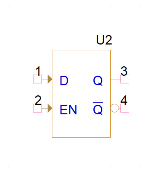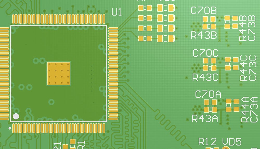
A PCB footprint is a precise layout of pads, outlines, and markings on a PCB that matches an electronic component’s physical dimensions and pin configuration. An accurate footprint enables correct component placement and soldering during assembly.
Not following PCB footprint design guidelines can lead to significant manufacturing and operation issues; including inaccurate pad dimensions and spacing that may cause solder bridging, a lack of compliance with manufacturer specifications and IPC standards, inadequate thermal reliefs for heat management, and/or misplaced or missing clear silkscreen markings for correct component orientation, just to name a few.
Avoid these design disasters with our PCB footprint design guidelines.
Step-by-Step PCB Footprint Design Guidelines
PCB footprint design guidelines specify how pads are arranged and the distance between them. To be most effective, footprint guidelines should include consideration for additional board attributes; such as the spacing of components, board edges, mounting holes, and other aspects of the PCB layout. These factors are reflected in the table below.
To ensure reliability and ease of assembly across multiple designs, you should follow best practices, such as maintaining consistency, cross-checking footprints with physical components, and keeping detailed documentation.
OrCAD Library Builder Is the Right Tool
PCB footprint accuracy is critical to ensure manufacturability and avoid contingencies during board development. An industry-leading PCB design tool like OrCAD Library Builder has the functionality to meet these requirements and streamline your PCB design process. Important features and capabilities include the following:
Automated Footprint Generation
- Standard Compliance: OrCAD Library Builder adheres to industry standards for generating accurate and reliable footprints.
- Footprint Wizard: The wizard guides users through a step-by-step process to create footprints based on component datasheets, reducing manual errors.
Efficient Data Management
- Centralized Library: It allows for a centralized library of components, ensuring that all team members use consistent and up-to-date components.
- Parameter Management: You can easily manage and update component parameters, ensuring accurate and current data across all designs.
Seamless Integration
- Integration with OrCAD PCB Designer: Footprints created in OrCAD Library Builder can be seamlessly integrated into OrCAD PCB Designer, ensuring a smooth design flow.
- Interoperability: The tool supports various file formats and can import/export data from different EDA tools, facilitating collaboration across different platforms.
Advanced Editing and Customization
- Custom Footprints: Users can create and customize footprints to meet specific design requirements.
- Graphical Interface: A user-friendly graphical interface allows for easy editing and visualization of footprints.
Quality Assurance
- DRC and Verification: Built-in Design Rule Checking (DRC) and verification tools help ensure that footprints meet design and manufacturing requirements.
- Error Minimization: Automated checks and validation processes reduce the risk of errors in the PCB design.
Library Migration and Management
- Legacy Data Support: It provides tools to convert and migrate legacy libraries to the OrCAD format, preserving valuable design data.
- Library Synchronization: Keep libraries synchronized across different projects and users, maintaining consistency.
Enhanced Productivity
- Time Savings: Automated processes and wizards save significant time compared to manual footprint creation.
- Efficiency: Streamlined workflows and easy-to-use tools improve overall design efficiency.
When manual PCB footprint creation is necessary, it is essential that important PCB footprint design guidelines are followed and implemented. Due to its range of capabilities and functionalities, OrCAD Library Builder provides one of the best solutions for board design and development efficiency. When incorporating this tool or other advanced software support products, partnering with an industry expert who can assist you in leveraging these tools effectively is the best option.
EMA Design Automation is a leading provider of the resources engineers rely on to accelerate innovation. We provide PCB design and analysis packages, custom integration software, engineering expertise, and a comprehensive academy of learning and training materials. For more information on PCB footprint design guidelines and how we can help you or your team innovate faster, contact us.