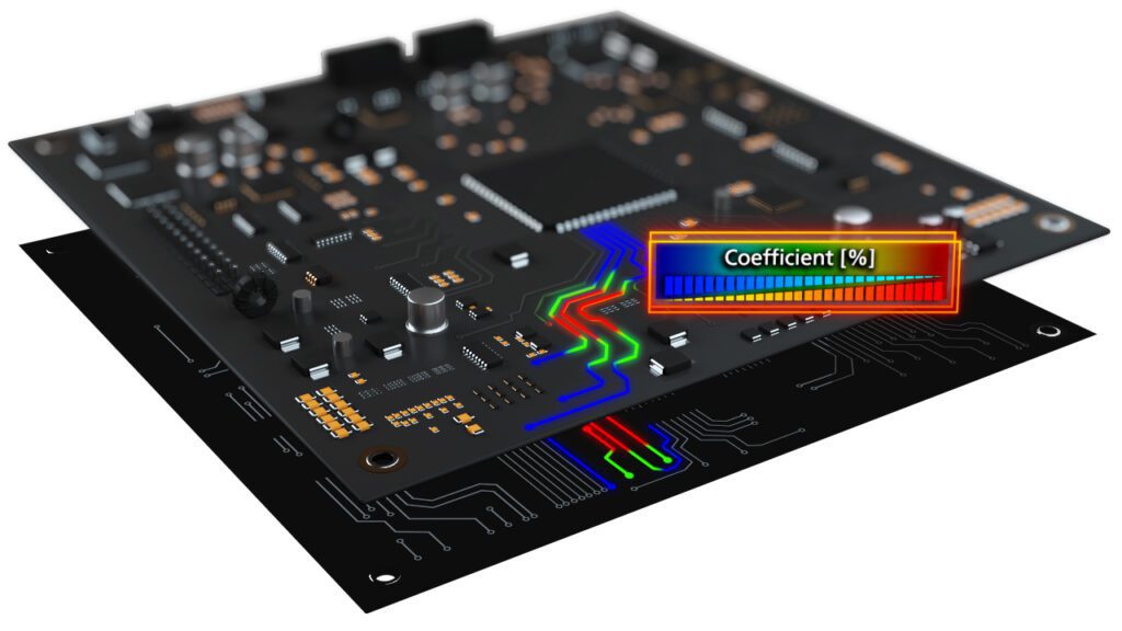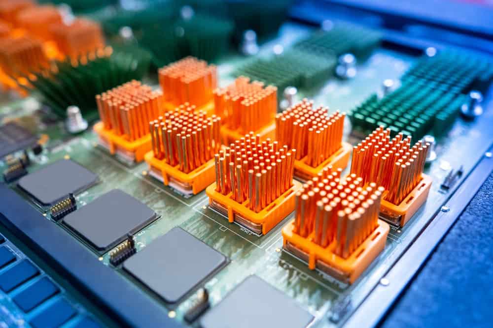
Designing PCBs for high-current applications presents challenges in heat management, trace width, and reliable connections. The high current generates significant heat, which must be effectively dissipated to avoid damage, performance issues and/or physical harm. This often requires thicker copper layers, wider traces, and additional thermal management solutions like heat sinks or thermal vias. Ensuring the PCB can handle high current without excessive voltage drops or electromagnetic interference (EMI) is crucial, which necessitates careful planning of the trace layout and grounding schemes.
PCB Design for High Current: A Balancing Act
Balancing these factors while maintaining manufacturability and cost-effectiveness is a complex task that requires careful design considerations. The table below provides more detailed information about PCB design for high current, including challenges and solutions.
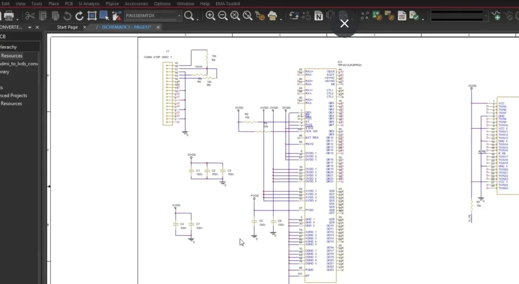
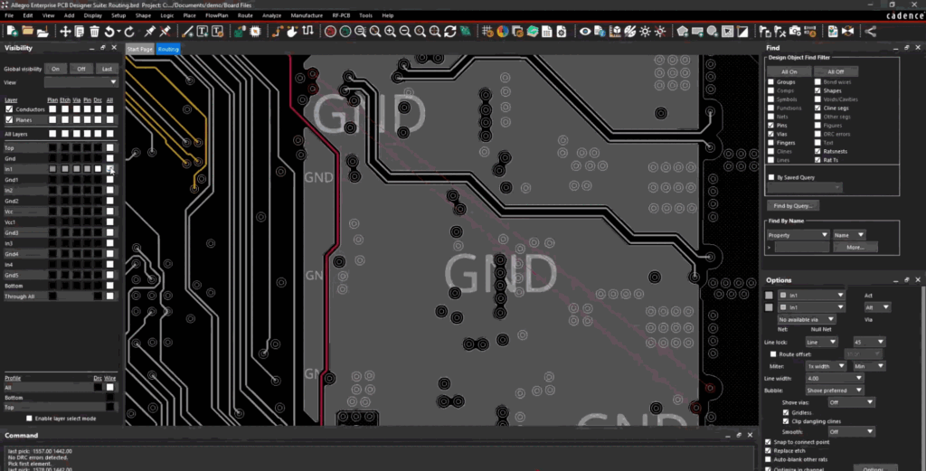
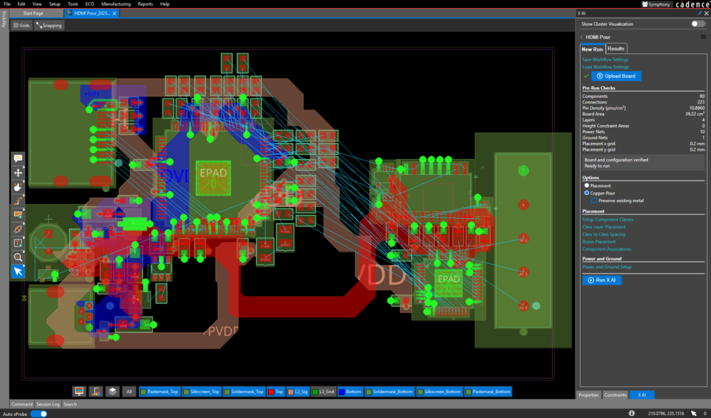
Each of the advanced design software tools listed above were specifically developed to target one or more areas during the PCB design stage to improve the overall electronic product development process.
| PCB Design for High Current: Challenges and Solutions | ||
| Factor | Challenge | Solution |
| Thermal Management | High current generates significant heat, which can damage components and degrade performance. | – Use wider and thicker copper traces – Implement thermal vias and heat sinks – Use PCB materials with high thermal conductivity |
| Voltage Drop | High currents can cause significant voltage drops across PCB traces, affecting performance. | – Minimize trace lengths – Use low-resistance materials – Employ a star grounding approach to ensure even distribution |
| Current Capacity | Ensuring traces can carry the required current without excessive heating or voltage drop. | – Calculate appropriate trace widths using IPC-2221 standards – Use multiple layers for power distribution – Use bus bars or heavy copper PCBs |
| Electromagnetic Interference (EMI) | High currents can generate EMI and electromagnetic compatibility (EMC) issues, interfering with nearby signals and components. | – Use ground planes to shield sensitive areas – Keep high-current traces away from signal traces – Implement proper filtering and decoupling |
| Power Distribution | Efficiently distributing power across the PCB without creating hot spots or uneven current distribution. | – Use multiple power and ground planes – Design with a solid ground plane for uniform distribution – Employ power polygons |
| Connector and Via Reliability | High currents can cause connectors and vias to overheat or fail, leading to poor connections. | – Use high-current-rated connectors – Increase the number and size of vias to distribute current more evenly |
| Material Selection | Standard PCB materials might not withstand the thermal and electrical stress of high-current applications. | – Use high-temperature and high-performance materials – Consider heavy copper or metal core PCBs for better durability |
| Signal Integrity | Maintaining signal integrity in high current can be challenging, especially for mixed-signal designs. | – Separate high-current paths from sensitive signal traces – Use differential signaling and proper termination techniques |
| Safety | High currents can pose safety risks, such as fire hazards or electric shocks. | – Ensure proper insulation and spacing according to safety standards – Implement fuses and circuit breakers for overcurrent protection |
| Mechanical Stress | High current paths might cause mechanical stress on the PCB, leading to potential cracking or delamination. | – Reinforce high-current areas with additional mechanical support – Avoid sharp bends in traces |
| Manufacturability | Designing for high currents complicates the manufacturing process, leading to increased costs or production issues. | – Collaborate with PCB manufacturers early in the design process – Adhere to design for manufacturability (DFM) guidelines to ensure ease of production |
High-Current PCB Applications

PCB design for high current is essential for various applications where robust and reliable power delivery is required. Some notable applications include:
| High-Current PCB Applications | |
| Application | Description |
| Electric Vehicles (EVs) | High-current PCBs are critical in EV powertrain systems, including battery management systems, motor controllers, and charging systems, where they handle significant power levels. |
| Power Supply Units (PSUs) | Used in computers, industrial equipment, and consumer electronics, PSUs require high-current PCBs to manage and distribute power efficiently. |
| Industrial Automation | Machinery and robotic systems in manufacturing processes often require high-current PCBs to power motors, actuators, and control systems, ensuring reliable operation under heavy loads. |
| Renewable Energy Systems | Solar inverters and wind turbines rely on high-current PCBs to convert and manage power from renewable sources, ensuring efficient energy transfer and storage. |
| Medical Equipment | MRI machines, X-ray machines, and other diagnostic tools require high-current PCBs to handle the substantial power needed for their operation and ensure patient safety and equipment reliability. |
| Telecommunications Infrastructure | Base stations and data centers use high-current PCBs in their power distribution networks to support the demanding electrical loads of servers and networking equipment. |
| Aerospace and Defense | High-current PCBs are used in radar systems, communication devices, and other critical systems that demand robust power handling capabilities and high reliability in extreme conditions. |
For the best results, you should partner with an industry expert to assist you in selecting the right software solution that is effective in incorporating these PCB design guidelines and integrates with your EDA software. With decades of industry expertise, EMA Design Automation is ready to help you with the tools, service, and support you need to meet your design goals.
EMA Design Automation is a leading provider of the resources engineers rely on to accelerate innovation. We provide PCB design and analysis packages, custom integration software, engineering expertise, and a comprehensive academy of learning and training materials. For more information on PCB design for high current and how we can help you or your team innovate faster, contact us.