The PCB design process is at once scientific and artistic. The best board designers are able to blend their creativity with proven technical principles to develop unique solutions that achieve desired performance objectives. It is informative to view design as the integration of synthesis–an overarching design intent perspective–with analysis, where aspects of the design are evaluated individually. To ensure operational reliability, it is important to understand the different types of PCB design analysis and how to best perform them for your project.
Types of PCB Design Analysis
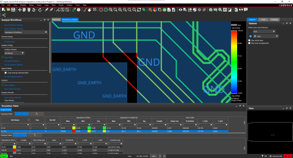
There are dedicated PCB design analysis software tools available, with leading EDA companies often having multiple analysis program options available. Most of these options fall under one of the types listed below.
The list above includes analyses that can be performed during schematic capture or PCB layout. By making design corrections and refinements prior to manufacture you can avoid costly redesigns and unnecessary board respins, and significantly minimize the possibility of operational problems that can lead to board failures and/or recalls.
Effective PCB Design Analysis Implementation
For DFM/DFA analysis, your EDA software likely includes functionality to perform PCB design analysis. In other cases, however, it may be necessary to employ a support program that directly addresses your specific analysis type need or has required advanced capabilities. The following are industry-leading software tools:
In order to maximally leverage the efficiency advantages of instituting analysis software, it is best to follow guidelines, as listed below.
Guidelines for Effective PCB Design Analysis Use
✅ Determine the specific analysis type(s) needed.
The most important attribute of a design analysis tool is that it aligns explicitly with the types of issues you need to address.
✅ Evaluate available analysis support options.
To ensure alignment with your specific issue(s), it is best to evaluate options;
including analysis engines and CAD format compatibility.
✅ Select an analysis software tool that integrates with your EDA program.
Employing third-party software can require substantial ramp-up time. Therefore, it is important that integration is as seamless as possible. Also, ensure training and support materials are available.
✅ Choose a solution that is scalable.
To prevent having to reinvent a PCB design analysis solution, it is best to select a tool that will grow as your design needs evolve.
Incorporating PCB design analysis into your workflow can yield significant benefits; such as higher quality designs, reduced/elimination of redesigns, faster manufacturing turnaround time, quicker overall development and bring up. The result of these improvements will translate into more accurate and reliable circuit boards for your clients.
EMA Design Automation is a leading provider of the resources that engineers rely on to accelerate innovation. We provide solutions that include PCB design and analysis packages, custom integration software, engineering expertise, and a comprehensive academy of learning and training materials, which enable you to create more efficiently. For more information on PCB design analysis options and how we can help you or your team innovate faster, contact us.