A well-optimized PCB design flow improves product performance, reduces manufacturing costs, and accelerates time-to-market. By carefully considering factors like signal integrity optimization, thermal management, design for manufacturability (DFM), and other PCB design flow parameters, designers can prevent costly redesigns, enhance product reliability, and ensure that the final product meets performance expectations. A streamlined design process also enables faster iteration and adaptation to changing market demands.
PCB Design Parameters for Design Flow Optimization
The table below examines important PCB design parameters for optimizing PCB design flow.
PCB Design Parameters for Optimizing PCB Design Flow | ||
Parameter | Description | Importance |
| Board Size and Shape | Dimensions and outline of the PCB | Determines the overall layout and component placement and affects the cost of the PCB. It must fit within the intended device and accommodate all components. |
Layer Count | Number of conductive layers | Affects the complexity, cost, and signal integrity. More layers allow for better routing and isolation of signals but increase cost and manufacturing complexity. |
Material Selection | Types of substrates and materials used | Influences the electrical performance, thermal properties, and cost. Different materials are chosen based on the application, such as high-frequency or high-temperature requirements. |
Trace Width and Spacing | The width of the conductive paths and the spacing between them | Critical for signal integrity, current carrying capacity, and manufacturability. Proper trace width and spacing help prevent short circuits and ensure reliable signal transmission. |
Component Placement | Arrangement of components on the board for optimal functionality | Affects the board’s performance, manufacturability, and thermal management. Proper component placement reduces signal path lengths, improves cooling, and simplifies assembly. |
Thermal Management | Heat dissipation strategies, such as heatsinks and thermal vias | Ensures components operate within safe temperature ranges, preventing damage and ensuring reliability. Effective thermal management is crucial for high-power and densely packed designs. |
Via Types and Sizes | Vias connect different layers and are crucial for routing signals and power. The choice of via type and size impacts the design’s complexity, cost, and electrical performance. | |
Signal Integrity | Techniques to minimize noise and signal degradation | Critical for high-speed and high-frequency designs. Good signal integrity practices prevent issues like crosstalk, reflection, and signal loss, ensuring reliable communication. |
Design for Manufacturability (DFM) | Guidelines to ensure the PCB can be manufactured efficiently and cost-effectively | Ensures the design can be produced with standard manufacturing processes, reducing costs and production time. DFM considerations help avoid issues like poor yield or long production lead times. |
Design for Testability (DFT) | Features that make the board easier to test post-production | Facilitates easier and more comprehensive testing of the PCB, improving quality and reliability. DFT features can reduce testing time and costs. |
Electromagnetic Compatibility/Electromagnetic Interference (EMC/EMI) Considerations | Strategies to minimize electromagnetic interference and emissions | Essential for regulatory compliance and to avoid interference with other devices. Good EMC/EMI practices prevent unintentional emissions and susceptibility issues. |
Design Rule Checks (DRC | Automated checks to ensure the design meets all specified rules | Ensures the design adheres to manufacturing, electrical, and mechanical constraints. DRC helps catch errors early, reducing costly revisions. |
PCB Design Flow and OrCAD X
OrCAD X, Cadence’s latest iteration of the OrCAD suite, offers a comprehensive solution for PCB design and analysis. It improves schematic capture and PCB design flow by integrating advanced features that streamline the process, optimize designs, and address supply chain challenges. Here’s how OrCAD X achieves these goals:
Enhanced Design Automation and Efficiency
- Schematic Capture and Layout Integration: OrCAD X provides a tightly integrated environment for schematic capture and PCB layout. Integration ensures seamless data transfer and consistency between design stages, reducing manual errors and saving time.
- Advanced Automation Tools: The suite includes automation tools for tasks such as component placement, routing, and DRC. These tools help speed up the design process, allowing designers to focus on more complex design aspects rather than routine tasks.
Scalability and Flexibility
- Customizable Workflows: OrCAD X offers customizable workflows that can be tailored to the specific needs of different projects, which allows teams to optimize their design processes and improve overall efficiency.
- Cloud Integration: The suite’s integration with cloud services enables remote access, collaboration, and data sharing, which is valuable for distributed teams and reduces time-to-market by enabling concurrent work.
- Software Solution that Scales with Your Needs: OrCAD X offers a unified PCB design environment allowing you to increase your features and capabilities as your design requirements evolve, without learning a new UI or software.
Supply Chain Optimization
- Real-Time Component Data Access: OrCAD X can access real-time component data, including availability, pricing, and lead times. This feature allows designers to make informed decisions early in the design process, selecting readily available and cost-effective components.
- Bill of Materials (BOM) Management: The software provides comprehensive BOM management capabilities, helping to ensure that all necessary components are accounted for and available.
- Lifecycle Management: OrCAD X can track component lifecycles, alerting designers to potential issues with end-of-life or obsolete parts. This proactive approach helps mitigate supply chain risks by ensuring that components will be available throughout the product’s lifecycle.
Error Detection and Correction
- Design Rule Checks: OrCAD X includes robust DRC capabilities to automatically detect and flag design rule violations, such as clearance issues, net connectivity errors, and other potential problems that could affect the PCB’s functionality or manufacturability.
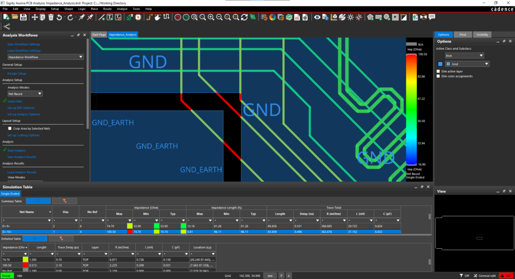
- Signal Integrity and Simulation: The suite offers advanced simulation tools for signal integrity, power integrity, and thermal analysis. These tools allow designers to simulate and analyze their designs before fabrication, identifying and correcting potential issues such as signal degradation, power distribution problems, or thermal hotspots.
- Integrated Debugging and Issue Tracking: OrCAD X integrates debugging tools and issue-tracking systems. This integration facilitates the identification, documentation, and resolution of design issues, ensuring a smoother design process and reducing the likelihood of errors reaching production.
Collaboration and Documentation
- Collaborative Tools: OrCAD X includes features that enable collaboration among design team members, such as shared design views, commenting, and version control. These tools help ensure that all team members are on the same page and can efficiently address any issues.
- Comprehensive Documentation: The software can generate detailed documentation, including assembly drawings, fabrication data, and test plans. This documentation is essential for ensuring the PCB can be manufactured and assembled correctly, reducing the risk of errors and rework.
OrCAD X improves the PCB design flow by providing powerful tools for design automation, error detection, and supply chain management. It helps designers create optimized, manufacturable designs while addressing common challenges such as component availability and design errors. By integrating advanced simulation, real-time data access, and collaborative features, OrCAD X offers a comprehensive solution that supports efficient and reliable PCB design and production.
For the most efficient integration of advanced tools like OrCAD X into your workflow, you should partner with an industry leader like EMA Design Automation, a Cadence Channel Partner serving all of North America, that specializes in furnishing engineers with advanced software tools and training
EMA Design Automation is a leading provider of the resources that engineers rely on to accelerate innovation. We provide solutions that include PCB design and analysis packages, custom integration software, engineering expertise, and a comprehensive academy of learning and training materials, which enable you to create more efficiently. For more information on PCB design flow optimization and how we can help you or your team innovate faster, contact us.


