The drive for faster throughput, increased mobility, and maximum efficiency in modern electronic devices has made power delivery a critical piece of design success. However, meeting the power needs of modern designs is anything but simple. To achieve a robust design, each supply must be capable of delivering sufficient current to every dependent device. In addition, those supplies must be both stable (able to maintain narrow voltage tolerances) and responsive (capable of adapting to transient current demands). Identifying and resolving power delivery problems late in the design process is incredibly difficult. If design power requirements aren’t considered upfront it can lead to schedule delays and a significant amount of debugging time in the lab. Implementing a power-driven, PCB layout methodology ensures the design process addresses critical power and signal integrity issues collectively at a time they can be easily solved.
Power Deliver Network (PDN), Power Integrity, Return Path Analysis, and many new terms are evolving, but ultimately it’s the same plane layers, copper pours, and “heavy” etch that has been part of the layout process for decades. What’s different now is tolerances we once could get away with can now ruin a product, potentially preventing its release and sales. The good thing is best practices combined with a solid understanding of your power system can be incorporated into your PCB design efforts to achieve a successful PDN and therefore a successful PCB.
Incorporate Power from the Beginning with Floor-planning
Much of the challenges product design teams face daily involve “tradeoff” decisions—the choices we make have unintended consequences: sometimes helpful, sometimes harmful. For example, improving the durability, makes things heavier. While changing materials could overcome this, it may come at the expense of product cost. Tradeoff decisions are often made in the early stages of PCB design, as this is where achieving a balance between competing disciplines (i.e., Mechanical, Thermal, Power, Compliance, Manufacturing, and others) should take place.
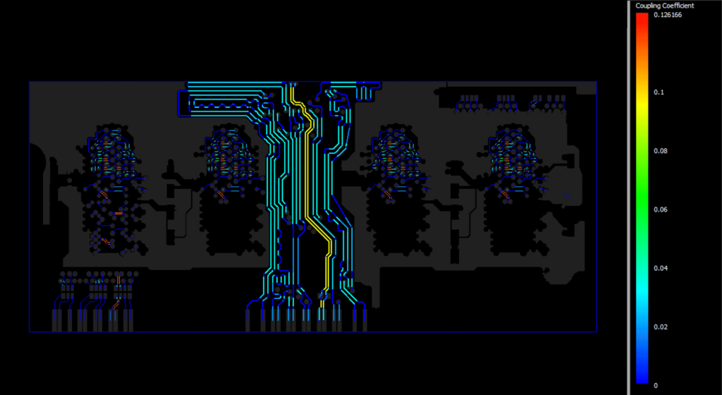
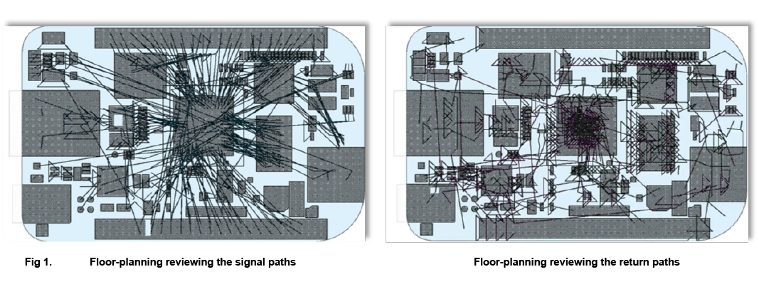
Floor-planning, the PCB designer engineers version of the block diagram, is done with varying degrees of formality on every PCB design. It’s a continuous process refined throughout layout, each time a new input is received, or some other discovery made. Floor-planning was largely used to ensure component placement adhered to mechanical constraints, however disciplines such as Thermal and Signal Integrity have found it is the best mechanism to convey their design requirements. Power considerations incorporated at the beginning of the PCB design, during floor-planning are key. To effectively perform “power-aware” floor-planning it is important to understand how the PDN operates, and specifically how energy is propagated through the PDN as this is the source of most confusion and problems.
Managing Propagation for Your PDN – Different than SI
It is often thought the energy supplied by the PDN is a continuous, steady stream of current at a particular DC voltage. However, in reality, the current in and out of a device can be represented by current bursts, synchronized by the rate each signal is switching. These current bursts can accumulate and act collectively, creating traffic-like conditions which may result in an unsustainable demand in the copper. In past designs much of the data transitions were coordinated via a central clock, however, today numerous, uncoordinated frequencies simultaneously transmit data creating unpredictable interactions among the frequencies.
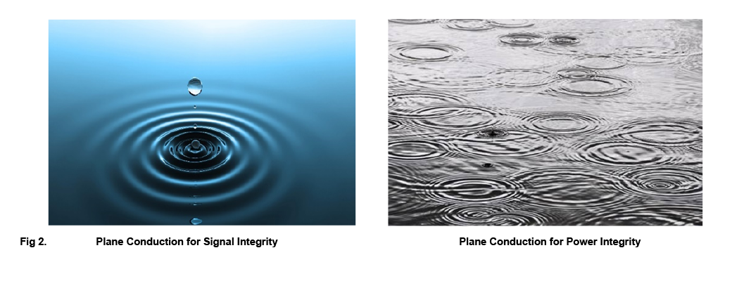
Unlike Signal Integrity models where the propagation direction is known, Power Integrity propagates in all directions when energy is injected on a copper plane or shape. This propagation is not without complication. Multiple signals of various frequencies, originating from different locations all exist simultaneously and all can interact both constructively and destructively making it nearly impossible to predict the conditions at any given location.
To address this, we use the frequency domain when modeling the behavior of the copper associated with the Power Delivery Network (PDN). A deeper understanding would reveal this is not limited to just the switching frequency but is applicable to non-sinusoidal signals as well. In fact, ANY signal can be decomposed to a sequence of repeating sine waves thru a process called transformation.
When looking at the images above (Fig. 2), it’s not hard to infer the difficulty one would face trying to predict the activity on the power planes the same way they would for traces during signal integrity simulation. Fortunately, we don’t have to. Referring to our newfound knowledge that any injected signal can be decomposed into a collection of sine waves, so to can the resulting collective plane noise. The implication being, if we can suppress the “ripples”, essentially targeting the frequencies that combine to form our noise, we can solve any power plane noise issue without knowledge of the source. Fortunately for us there is a readily available tool to help us do just that … the capacitor.
Capacitors: Our Most Valuable PDN Asset
With most of our attention reserved for routing the copper (rightfully so) it’s easy to overlook our most valuable PDN asset, the capacitor. We’ve all seen them. They’re everywhere, but what do they do?
The answer is twofold, but surprisingly simple. First, they resist voltage changes, acting like a “shock absorber” holding the voltage across its pins steady. Second, they provide “reserve energy” in effect, creating localized storage around the board capable of responding to instant demands for transient power.
Capacitors suppress voltage ripples and are effective on both Power and Ground due to their inherent resistance to voltage change. Noise that would otherwise propagate in all directions on the power plane is suppressed or reduced in amplitude by the mere presence of the capacitor. However, they are not all equally effective in doing so. The extent to which a capacitor can “smooth” noise on the plane is controlled by both the device itself and the way in which it is attached to the PCB.
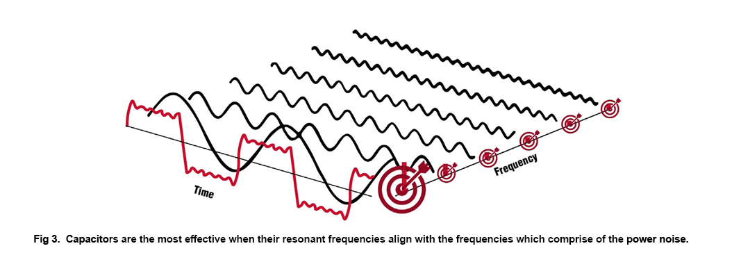
Fig 3. Capacitors are the most effective when their resonant frequencies align with the frequencies which comprise of the power noise.
Each capacitor has a particular frequency at which it provides its greatest suppression ability. Known as “resonant frequency”, and seen in the figure below at the valley, the resonant frequencies are used to target those frequencies encountered on the PDN.
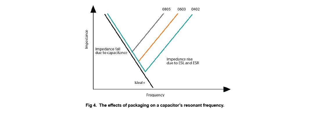
Fig 4. The effects of packaging on a capacitor’s resonant frequency
When using capacitors in your power delivery network, several factors can influence the value of the resonant frequency: package size, placement, and manufacturer and materials. Careful capacitor selection should be employed to ensure the plane voltage remains stable as PDNs evolve. All capacitors are not created equal and as power requirements increase the need to understand and carefully deploy your capacitors is more important that ever.
Power Drives Design Success
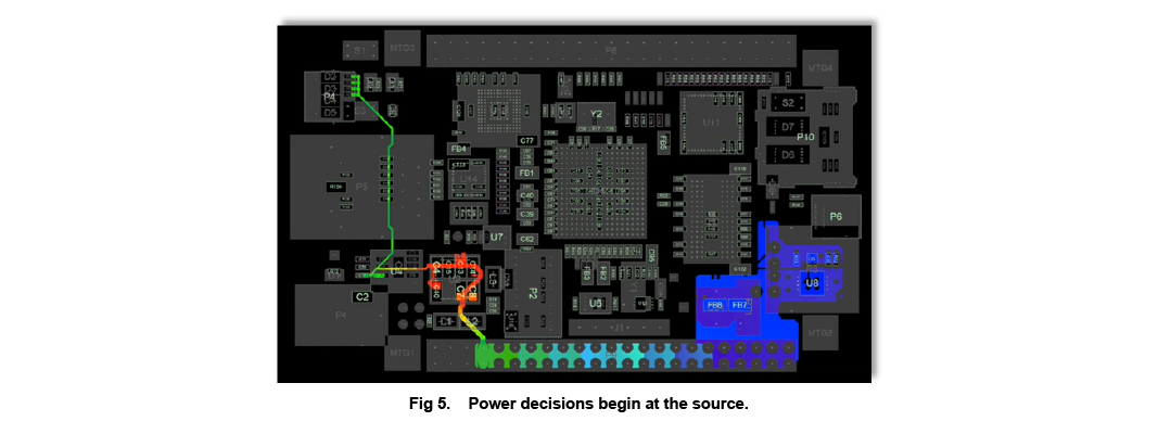
Fig 5. Power decisions begin at the source.
Power drives your design, influencing every choice made. With the increasing complexity of the power delivery network due to technological advancements, every choice is now critical to overall design success and board functionality. Therefore, it is imperative to consider power throughout the design process. This can be achieved through proper floor-planning, using the frequency domain to model behavior, and careful component selection and placement. Implementing these best practices of PDN design ensures critical power and signal integrity issues are addressed collectively as you design.