The Internet of Things (IoT) is one of the fastest growing markets in the world right now. Currently there are over twenty-five billion IoT devices in the world and it is estimated that in the next ten years there will be over 100 billion IoT devices. This equates to around 10 to 12 devices for every human being on the planet by the year 2030.
As IoT continues to rise in popularity, the demand for Internet enabled electronic device hardware engineers are more important than ever. While many of these IoT devices are intended to “just work” and be as simple as possible for the end user, designing the electronics to achieve that result can be quite complicated. How does someone tackle designing IoT devices? We had the opportunity to chat with Rick Hartley, an expert engineer with over fifty-five years in the field, to discuss the trends, common challenges, and solutions.
Common IoT Challenges
According to Hartley, there are a few common challenges in designing IoT to be on the lookout for: signal integrity and electromagnetic interference issues (EMI).
“The reality is devices and circuits today have become so fast that traces on circuit boards that are no longer than an inch or so become high speed transmission lines,” said Hartley. There is an increase in energy that compromises signal integrity and keeps the board from functioning properly. Finding a way to contain the energy produced is another challenge. If released, this energy will create EMI.
“It doesn’t matter where your product is going in the world, everybody has to pass certain standards and they have to be able to have their board tested and ensure that it will not give off more than a certain amount of energy,” said Hartley.
The IoT market has its own set of standards that must be met. To be able to design any type of IoT related circuit board, engineers must be able to meet these standards and overcome any SI and EMI challenges. Success is by no means ensured.
“One of the statistics I learned when researching the IoT market is 75 to 80 percent of people who start out to build a device fail and give up because they can’t make it work. That’s why design becomes so critically important,” said Hartley.
In a world where cost is everything, as it is in the IoT world, things such as signal integrity and EMI become extremely important. When cost is critical, manufacturability is critical. When asked about the loss of money from restarting projects, Hartley said the cost is enormous. “Every time you go into EMI testing, it’s about ten thousand dollars. If it takes two or three or even four respins, look at the money you’ve wasted,” said Hartley. “There’s a real value in getting things right the first time.”
Gaining the Skills for Design Success
So how does an engineer gain these skills? One way is through reading materials. “There are numerous books that talk about how to lay out circuit boards to avoid poor lay out issues,” said Hartley. He recommends Grounding and Shielding by Ralph Morrison, as well as the EMA e-book, The Hitchhiker’s Guide to PCB Design.
Hartley has continued to seek more knowledge throughout his career as an engineer. While working on a project in the late 80s, he ran into EMI issues and no one, including Hartley, understood why. “I had been in field service and spent four or five years installing circuitry, testing, and troubleshooting to find problems and figure out what was going on. I didn’t have a clue what was going on,” said Hartley. It wasn’t until close to ten years later that things clicked for him. “Once I was on the path or understanding what was happening, things started to come together.”
And is Hartley still figuring these things out? “It’s a never-ending process. If you aren’t constantly learning, you’re not keeping up.”
IoT and PCB Design Layout Webinar
Another way to gain better insight into IoT design is a PCB2Day webinar class hosted by Hartley himself. Students of the webinar can expect to walk away with the knowledge of how to design a low-layer board that functions properly the first time. They will also earn how to pass EMI testing at a low cost.
“I will try to impart enough information to give them the knowledge and to give them a reason to seek more knowledge,” said Hartley. “It’s very challenging to get a circuit board with high speed devices on it to function properly in one, two, and four layers unless you really understand how to lay out the circuit boards. And that’s really what this class is going to focus on.”
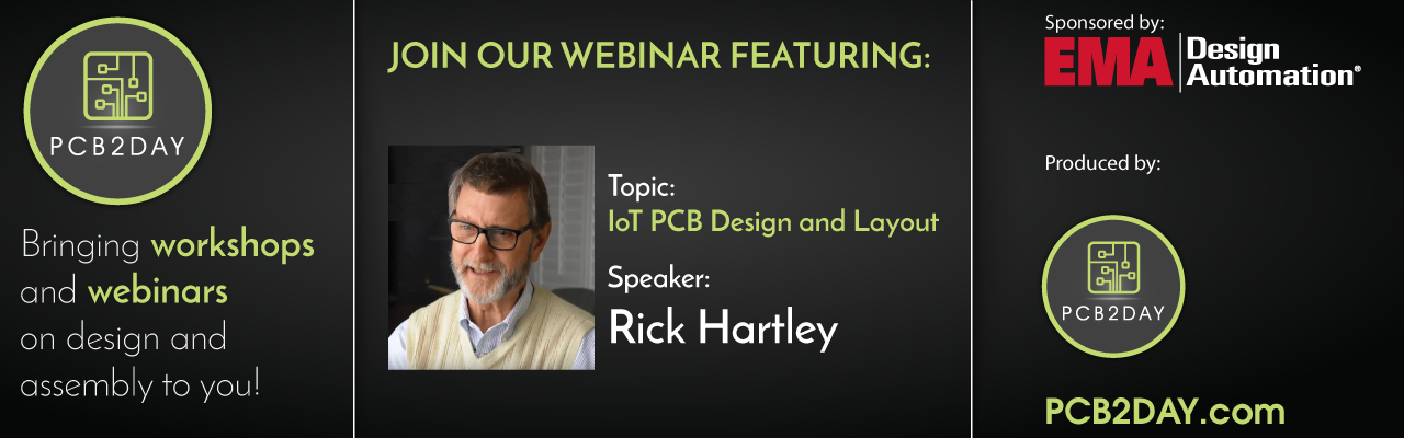
For more information and sign up for Rick’s webinar on June 25th: https://zoom.us/webinar/register/8915907776065/WN_bFuW1oUJQbyZVdLB7_GBjQ
About Rick Hartley – Rick Hartley, a retired senior principal engineer at L-3 Avionics Systems, is principal of RHartley Enterprises, through which he consults and teaches internationally. His focus is on correct design of circuits and PC boards to prevent and/or resolve EMI, noise and signal integrity problems. He has consulted with major corporations in the US and 14 other countries. His career has focused on computers, telecommunications, and aircraft avionics, as well as medical, automotive and appliances. He has taught seminars at numerous conferences, including the IEEE EMC Symposium, PCB West, IPC Apex Expo and others. He is on the board of directors of the Printed Circuit Engineering Association, a past member of the Editorial Review Board of Printed Circuit Design magazine and has written numerous technical papers and articles on methods to control noise, EMI and signal integrity.