As technology trends towards smaller, faster, cheaper, the challenges around good PDN design are getting more difficult. With multiple requirements needed from many disciplines, the demands of the PDN are only going to increase and become harder to maintain.
Over the past few months, we have discussed important elements that are essential to power delivery and PDN requirements. Now that we have a better understanding of this, it’s time to explore what is needed to create the ideal PDN product and who is best equipped to bring all the elements of the PDN together.
What is a good PDN design and how do you achieve it?
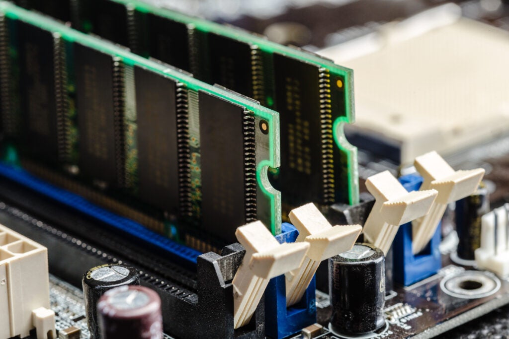
Power-related design objectives tend to be similar in nature for all PCBs: to provide sufficient current at a stable voltage to each device. However, what does vary widely is complexity. They can range from simple, single-supply, powering a solid power plane to a multi-source, hot-swappable, self-monitoring, thermally sensitive, complex design that accounts for most components and a large amount of copper on the PCB. Simply put, a good PDN design is one that delivers power adequately and reliably however, achieving this is not as simple as it sounds. There are multiple disciplines and requirements that play a role in the success of the PDN, and ultimately, product functionality. These requirements influence other design decisions and if not considered at the right time, can be almost impossible to address as the process moves forward. The PDN design, both parts and etch, typically are the most difficult to change.
PDN parts, particularly magnetics, filters, and regulator-type devices often come with placement guidelines from different disciplines which can be conflicting and may ultimately need mediation. While never an advocate of the cookie cutter approach, my advice, wherever possible is to Route Power First. Circulate it, review it, involve the other disciplines, and seek agreement. Use it for the canvas as you floorplan. Power problems are echoed on every signal on the rail and they’re a nightmare to fix.
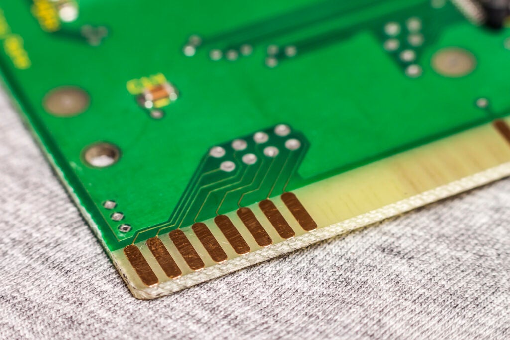
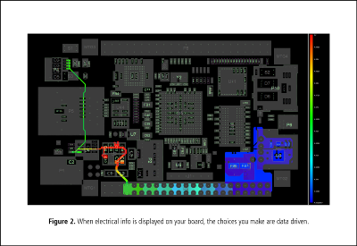
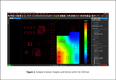
In addition to the power delivery role, the PDN also typically carries the return current associated with the digital signals on the board. As a result, the copper shapes of the power nets are often influenced by adjacent signal routing, being reshaped to provide an uninterrupted return plane above and/or beneath routed trace. It is important to “size” the copper (i.e., define shapes & vias) based on simulated current density and voltage drop. This “best practice” can be achieved through visual inspection or with simulation tools.
Experienced design teams recognize solving power-related problems always involve “multi-physics” trade-offs, such as placing components far enough to allow the heat to dissipate, but close enough to meet EMI requirements. This is in addition to any contributing factors which provide additional limits. For example, placing devices as close as possible for optimal signal integrity but not too close to be re-worked.
Therefore, the PDN needs to be addressed as a system. Each individual power net, even if routed with exceptional precision, can be compromised if demands aren’t properly considered. Additionally, each net in the power system must be capable of delivering adequate DC current on its own, while limiting its losses to an acceptable level (voltage drop). Individually, the nets must also be able to deliver that current not just in adequate quantity, but with the necessary responsiveness such that the voltage is stable, even to high-speed transients.
Like a plumbing system, we must ensure each pipe is sized to handle the flow. Not only does this pipe need to handle its own requirements, but it must also account for the requirements of the additional sources connected to it. To achieve our DC goal, we need to approach the PDN design similarly. Therefore, before making important layout decisions, we must consider the requirements of adjacent disciplines such as thermal, EMI, mechanical constraints, safety, etc. to give us the best possible chance at first-pass success (as all will affect the PCB layout).
Opportunity Knocks
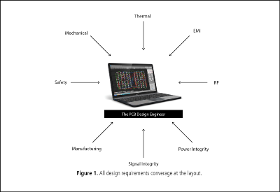
Everybody has a hand in the PDN, but nobody owns it, unless you have an in-house power integrity engineer. Everyone cares about their own design requirements, but there is no one owning how they all come together. It’s this lack of ownership that is the root of many PDN design issues. Each of the disciplines involved in product development have requirements that must be met and are often determined far too late in the design cycle. For better or worse, all requirements will collide at layout.
The PCB design engineer must either meet or manage every requirement for all disciplines making them best positioned to manage the PDN design. The impact of the PDN on the traditional PCB design process can enhance our ability to make informed decisions. For example, consider the task of splitting a plane to contain two distinct voltages. Now reconsider this knowing one of those nets carries nearly the full current of the power supply and the other carries but a trickle. With this knowledge, plane cuts would be different, effecting overall board performance.
Within the design process, every action has a multi-effect that needs to be balanced and as time goes on, its importance will increase. Someone needs to take on the role of managing these actions and the PCB design engineer is the best person to do so. PCB design engineers understand how to balance design requirements with manufacturability and have the most influence over the success of the PDN. The multitude of tools available directly within the PCB canvas enables PCB design engineers to seamlessly incorporate both signal and power integrity within their design process while minimizing time concerns.
The PDN is Evolving, We Must Evolve with It
We’ve always had power, so what’s different now? The PDN is evolving, and margins are shrinking. Operating voltages dropping from 1.8 to 1.5 and then 1.2 as the input current doubled for memory is a hallmark example of this evolution. As the complexity increases, not having an owner increases the potential for failure.
The PCB design engineer has the most influence when it comes to ensuring good power delivery as they control every element needed to build the PDN. The PDN is essentially a physical problem and while it can be planned early in the design process, full definition and realization doesn’t occur until the PCB layout.
Most companies don’t have the luxury of having a designated power integrity engineer. As the needs of PDN design are evolving, we must evolve with it. With the role of the electrical engineer morphing into the PCB designer, now is the ideal time to take this opportunity to incorporate power integrity with minimal disruption to the existing design process.
Contact us for more information on how Sigrity can be used to analyze signal integrity and power integrity for PCB Designers.